In the circuit shown below, a positive edge-triggered D Flip-Flop is used for sampling input
data Din using clock CK. The XOR gate outputs 3.3 volts for logic HIGH and 0 volts for
logic LOW levels. The data bit and clock periods are equal and the value of $${{\Delta T} \over {{T_{CK}}}}$$ = 0.15,
where the parameters $$\Delta T$$ and TCK are shown in the figure. Assume that the Flip-Flop and the
XOR gate are ideal.
If the probability of input data bit (Din) transition in each clock period is 0.3, the average
value (in volts, accurate to two decimal places) of the voltage at node X, is _______.
Your input ____
2
GATE ECE 2017 Set 2
Numerical
+2
-0
The state diagram of a finite state machine (FSM) designed to detect an overlapping sequence of three bits is shown in the figure. The FSM has an input 'In' and an output 'Out'. The initial state of the FSM is S0.
If the input sequence is 10101101001101, starting with the left-most bit, then the number of times 'Out' will be 1 is __________.
Your input ____
3
GATE ECE 2017 Set 1
MCQ (Single Correct Answer)
+2
-0.6
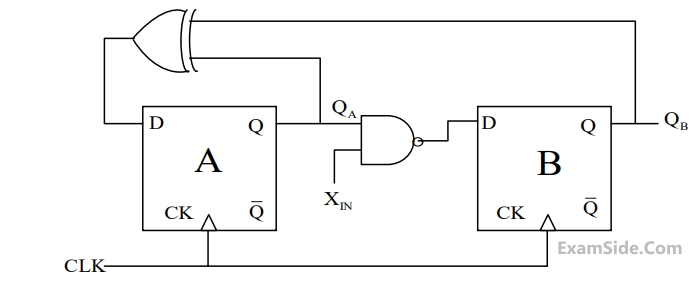
A finite state machine (FSM) is implemented using the D flip-flops A and B and logic gates, as shown in the figure below. The four possible states of the FSM are QA QB = 00, 01, 10, and 11.
Assume that XIN is held at a logic level throughout the operation of the FSM. When the FSM is initialized to the state QA QB = 100 and clocked, after a few clock cycles, it starts cycling through
A
all of the four possible states if XIN = 1
B
three of the four possible states if XIN = 0
C
only two of the four possible states if XIN =1
D
only two of the possible states if XIN = 0
4
GATE ECE 2017 Set 1
Numerical
+2
-0
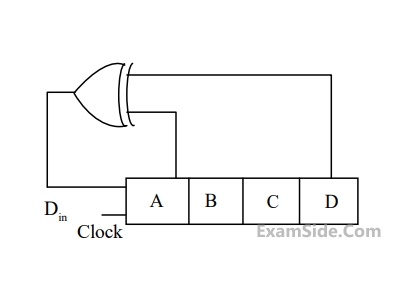
A 4-bit shift register circuit configured for right-shift operation is $${D_{in}}\, \to \,A,\,A\, \to B,\,B \to C,\,C \to D,$$ is shown. If the present state of the shift register is ABCD = 1101, the number of clock cycles required to reach the state ABCD = 1111 is