Sequential Circuits · Digital Circuits · GATE ECE
Marks 1
A binary ripple counter is designed to count $(0)_{10}$ to $(64)_{10}$. Which of the following is/are the number of flip-flops required to design the counter?
The negative edge triggered $J K$ flip-flop in the Figure has $J$ and $K$ inputs tied to Logic High and a square wave of 10 cycles/second is applied to its clock $(C)$ input. The frequency of the output $Q$ (in cycles/second) is $\_\_\_\_$ .
(rounded off to two decimal places)

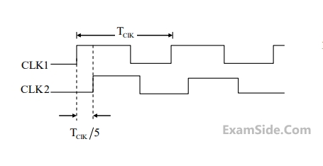
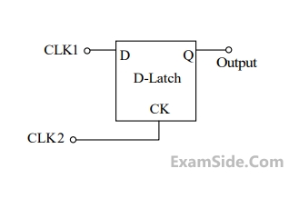
The synchronous sequential circuit shown below works at a clock frequency of 1 GHz. The throughput, in Mbits/s, and the latency, in ns, respectively, are

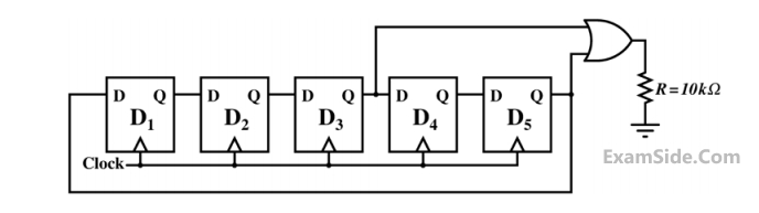
The average power dissipated (in mW) in resistor R is ______.


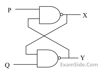
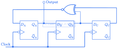
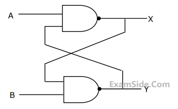
Which one of the following Boolean functions is realized by the circuit?


Group1
P. shift register
Q. Counter
R. Decoder
Group2
1. Frequency division
2. Addressing in memory chips
3. Serial to parallel data conversion


Marks 2
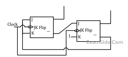
A shift-left Shift Register (SR) and a $D$ flip-flop are connected to a synchronized clock as shown in the Figure. Assume that the SR and D flip-flops are initially cleared and the XOR gate has no propagation delay.
Which of the following options gives the correct binary representation $\left(b_7 b_6 b_5 b_4 b_3 b_2 b_1 b_0\right)$ of the content of the shift register immediately after the $5^{\text {th }}$ clock transition (positive edge)?

A positive-edge-triggered sequential circuit is shown below. There are no timing violations in the circuit. Input $P 0$ is set to logic ' 0 ' and $P 1$ is set to logic ' 1 ' at all times. The timing diagram of the inputs SEL and $S$ are also shown below.
The sequence of output $Y$ from time $T_0$ to $T_3$ is $\qquad$ .

In the circuit shown below, the AND gate has a propagation delay of 1 ns . The edgetriggered flip-flops have a set-up time of 2 ns , a hold-time of 0 ns , and a clock-to-Q delay of 2 ns .
The maximum clock frequency (in MHz , rounded off to the nearest integer) such that there are no setup violations is___________ .

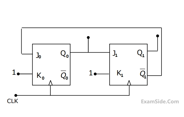
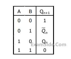
The sequence of states $(Q_1 Q_0)$ of the given synchronous sequential circuit is ________.
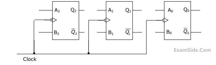
In a given sequential circuit, initial states are Q$$_1$$ = 1 and Q$$_2$$ = 0. For a clock frequency of 1 MHz, the frequency of signal Q$$_2$$ in kHz, is ___________ (rounded off to the nearest integer).

for the circuit shown, the clock frequency is f0 and the duty cycle is 25%. For the signal at the Q output of the Flip-Flop, ___________.

A state transition diagram with states A, B, and C, and transition probabilities p1, p2, ....., p7 is shown in the figure (e.g., p1 denotes the probability of transition from state A to B). For this state diagram, select the statements which is/are universally true.

The propagation delay of the exclusive-OR (XOR) gate in the circuit in the figure is 3 ns . The propagation delay of all the flip-flops is assumed to be Zero. The clock (Clk) frequency provided to the circuit is 500 MHz .
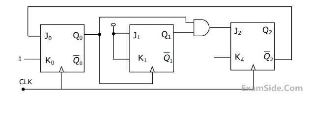
 Starting from the initial value of the flip-flop outputs $Q_2 Q_1 Q_0=111$ with $D_2=1$, the minimum number of triggering clock edges after which the flip-flop outputs $Q_2 Q_1 Q_0$ becomes 100 (in integer) is $\_\_\_\_$
For the components in the sequential circuit shown below, $t_{p d}$ is the propagation delay, $t_{\text {secup }}$ is the setup time and $t_{\text {hold }}$ is the hold time. The maximum clock frequency (rounded off to the nearest integer), at which the given circuit can operate reliably, is $\_\_\_\_$ MHz.

The state diagram of a sequence detector is shown below. State $S_0$ is the initial state of the sequence detector. If the output is 1 , then


If the probability of input data bit (Din) transition in each clock period is 0.3, the average value (in volts, accurate to two decimal places) of the voltage at node X, is _______.
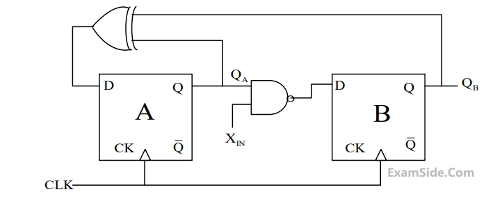
Assume that XIN is held at a logic level throughout the operation of the FSM. When the FSM is initialized to the state QA QB = 100 and clocked, after a few clock cycles, it starts cycling through

If the input sequence is 10101101001101, starting with the left-most bit, then the number of times 'Out' will be 1 is __________.

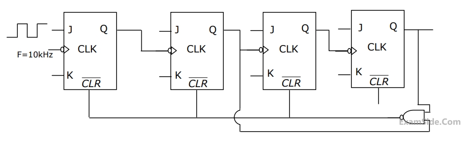
If the clock (Clk) frequency is 1 GHz, then the counter behaves as a

Which one of the following statements is correct?


Suppose the XOR gate is replaced by an XNOR gate. Which one of the following options preserves the state diagram?


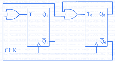
Which of the following waveforms correctly represents the output at Q1?


The inputs D0 and D1 respectively should be connected as


Marks 5
(a) Write down the state table for the mod-5 counter.
(b)Obtain simplified SOP expressions for the inputs A2, B2, A1, B1, A0 and B0 in terms of Q2, Q1, Q and their complements.
(c) Hence, complete the circuit diagram for the mod-5 counter given in the figure using minimum number of 2-input NAND-gate only.
(a) Will the counter lockout if it happens to be in any one of the unused states?
(b) Find the maximum rate at which the counter will operate satisfactorily. Assume the propagation delays of flip-flop and AND gate to be tF and tA
The Clock has a period of 50ns and transitions take place at the rising clock edge.
(a) Give the sequence generated at Q0 till it repeats.
(b) What is the repetition rate for the generated sequence?


One possible implementation of the state machine is shown figure. Specify what signals should be applied to each of the multiplexer inputs


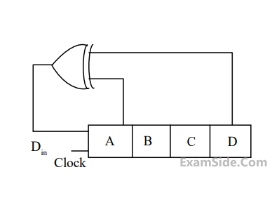
(a) Write the 4-bit values (Q0Q1Q2Q3) after each clock pulse till the pattern (1000) reappears on (Q0Q1Q2Q3).
(b) To what values should the shift register be intialized so that the pattern (1001) occurs after the first clock pulse?
Marks 8
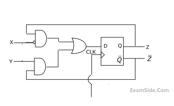
If XY=00, the flip-flop changes stage with each clock pulse.
If XY=01, the flip-flop state Q becomes 1 with the next clock pulse.
If XY=10, the flip-flop state Q becomes 0 with the next clock pulse.
If XY=11, no change of state occurs with the clock pulse.
(a) Write the Truth table for the X-Y flip flop
(b) Write the Excitation table for the X-Y flip flop
(c) It is desired to convert a J-K flip flop into the X-Y flip flop by adding some external gates, if necessary. Draw a circuit to show how you will implement the X-Y flip-flop using a J-K flip-flop.


For M=1, sequence of Q1, Q0 is ..00, 01, 10, 11, 00, 01.......
For M=0, sequence of Q1, Q0 is ..00, 11, 10, 01, 00, 11......
(a)Design the necessary feedback logic for T1 and T0.
(b)Realize the feesback logic using inverters and 4-input multiplexers only. Use Q1 and Q0 as the control inputs of the multiplexer with Q1 as the MSB.
