Operational Amplifier · Analog Circuits · GATE ECE
Marks 1
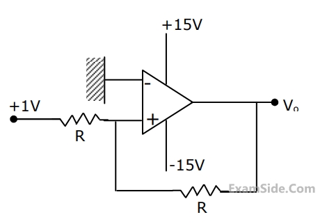
The ideal OP-AMP circuit shown in the Figure produces output voltage $V_o=x$ when the Switch, $S$, is open.
Which of the options represents the output voltage when S is closed?

Consider the circuit shown in the Figure with $V_i=3 \mathrm{~V}$ and $V_{c c}=12 \mathrm{~V}$. Assume $V_{B E}=0.7 \mathrm{~V}$ and $\beta_{\mathrm{dc}}=99$ for the BJT.
Which of the following options is the correct value of the current $I_o$ ?

An ideal OPAMP circuit with a sinusoidal input is shown in the figure. The 3 dB frequency is the frequency at which the magnitude of the voltage gain decreases by 3 dB from the maximum value. Which of the options is/are correct?

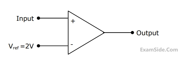
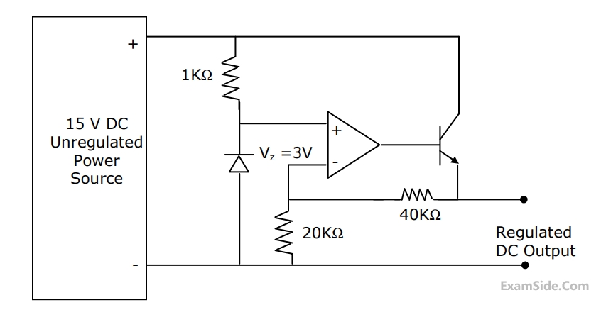
For the circuit with an ideal OPAMP shown in the figure. $V_{\text {REF }}$ is fixed.
 If $V_{\text {OUT }}=1$ volt for $V_{\text {IN }}=0.1$ volt and $V_{\text {OUT }}=6$ volt, for $V_{\text {IN }}=1 \mathrm{~V}$, where $V_{\text {OUT }}$ is measured across $R_{\mathrm{L}}$ connected at the output of this OPAMP. The value of $R_{\mathrm{F}} / R_{\text {IN }}$ is
Consider the circuit with an ideal OPAMP shown in the figure.
 Assuming $\left|V_{\mathrm{IN}}\right| \ll\left|V_{\mathrm{CC}}\right|$ and $\left|V_{\mathrm{REF}}\right| \ll\left|V_{\mathrm{CC}}\right|$. The condition at which $V_{\text {OUT }}$ equals to zero is
A circuit with an ideal OPAMP is shown in the figure. A plus $V_{\text {IN }}$ of 20 ms duration is applied to the input. The capacitors are initially uncharged.
 The output voltage $V_{\text {OUT }}$ of this circuit at $\tau=0^{+}$(in integer) is $\_\_\_\_$ V.
The components in the circuit shown below are ideal. If the op-amp is in positive feedback and the input voltage $V_i$ is a sine wave of amplitude 1 V , the output voltage $V_0$ is

In the circuit shown below, all the components are ideal. If $V_i$ is +2 V , the current $I_0$ sourced by the OpAmp is $\_\_\_\_$ mA .


The number of times the LED glows is ______.

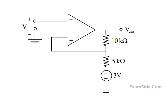
The load current I0 through RL is

The value of $${{{V_{OB}}} \over {{V_{OA}}}}$$ is _____


Marks 2
A circuit using an ideal OP-AMP is shown in the Figure.
Which of the following options gives the correct value of the current $I_\chi$ ?

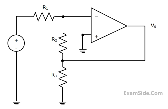
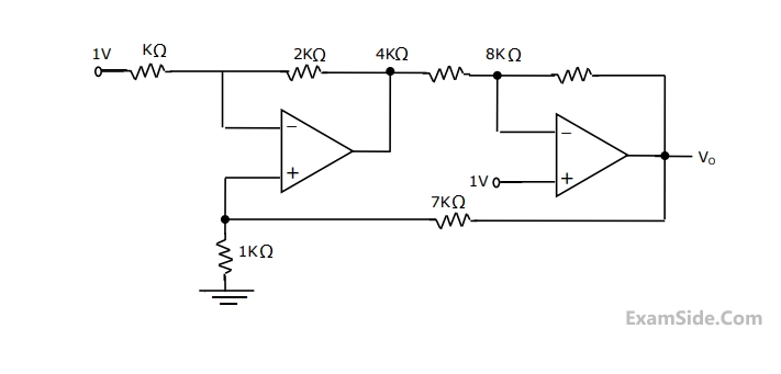
Consider an ideal OP-AMP circuit as shown in the Figure.
The resistances $R_1=R_2=R_3=R_4=50 \mathrm{k} \Omega$.
The magnitude of the closed loop gain is $\_\_\_\_$ . (rounded off to two decimal places)

The opamps in the circuit shown are ideal, but have saturation voltages of ±10 V.

Assume that the initial inductor current is 0 A. The input voltage (Vi) is a triangular signal with peak voltages of ±2 V and time period of 8 μs. Which one of the following statements is true?
In the circuit below, the opamp is ideal.

If the circuit is to show sustained oscillations, the respective values of $R_1$ and the corresponding frequency of oscillation are ____.
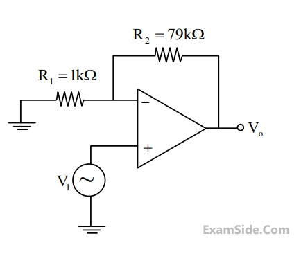
The $$\mathrm{{{{V_{OUT}}} \over {{V_{IN}}}}}$$ of the circuit shown below is

A sample and hold circuit is implemented using a resistive switch and a capacitor with a time constant of 1 $$\mu$$s. The time for the sampling switch to stay closed to charge a capacitor adequately to a full scale voltage of 1 V with 12-bit accuracy is ___________ $$\mu$$s (rounded off to two decimal places).
A circuit with an ideal OPAMP is shown. The Bode plot for the magnitude (in dB) of the gain transfer function (Av(j$$\omega$$) = Vout(j$$\omega$$)/Vin(j$$\omega$$)) of the circuit is also provided (here, $$\omega$$ is the angular frequency in rad/s). The values of R and C are __________.


The output voltage Vout (in volts) is _____.

The output voltage (in millivolts) is ________.

The time t = t1 (in seconds) at which Vo changes state is _____.


A triangular wave which goes from -12V to 12V is applied to the inverting input of the OP-AMP. Assume that the output of the OP-AMP swings from +15V to -15V. The voltage at the non-inverting input switches between.

and V is the voltage across the diode (taken as positive for forward bias). For an input voltage $${V_i}\,\, = \,\, - 1V,$$ the output voltage V0 is


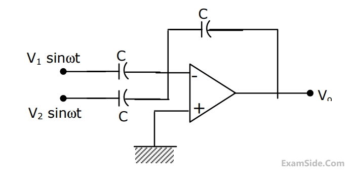
If $${V_i} = {V_1}\,\,\sin \left( {\omega \tau + \phi } \right),$$ then the minimum and maximum values of $$\phi $$ (in radians) are respectively

The transfer function $${V_o}\left( s \right)/{V_i}\left( s \right)$$ is

In the figure shown above, the OP-AMP is supplied with $$ \pm $$ 15V.


Marks 5

(a) Obtain an expression for V0 in terms of Vs, R, and the reverse saturation current Is of the transiostor.
(b) If R = 1$$\Omega $$, Is = 1pA and the thermal voltage VT = 25mV, then what is the value of the output voltage V0 for an input voltage Vs = 1V?
(c) Suppose that the transistor in the feedback path is replaced by a p-n junction diode with a reverse saturation current of Is. The p-side of the diode is connected to node A and the n-side to node B. Then what is the expression for V0 in terms Vs, R and Is ?

The characteristics of the diode are given by the relation I = Is $$\left[ {{e^{{{qV} \over {KT}}}} - 1} \right],$$
Where V is the forward voltage across the diode
(a)Express V0 as a function of Vi assuming Vi> 0.
(b)If R = 100K$$\Omega $$ , Is = 1$$\mu $$A and $${{KT} \over q}\,\, = \,\,25mV$$


when $${R_a}\, = \,{R_b}\, = \,{R_c}\,{R_d}\,$$ ohms.
when $${R_a}\, = \,{R_b}\, = {R_c}\, = 100$$ ohms and $${R_{d\,}}\, = \,120$$ ohms.

