Logic Families · Digital Circuits · GATE ECE
Marks 1
1
Select the correct statement(s) regarding CMOS implementation of NOT gates.
GATE ECE 2022
2
The output (Y) of the circuit shown in the figure is
GATE ECE 2014 Set 4
3
The full forms of the abbreviations TTL and COMS in reference to logic families are
GATE ECE 2009
4
The transistors used in a portion of the TTL gate shown in figure have β=100. the base-emitter voltage of is 0.7V for a transistor in active region and 0.75V for a transistor in saturation . If the sink current I=1mA and the output is at logic 0,
then the current $${I_R}$$ I will be equal to

GATE ECE 2005
5
Both transistors T1 and T2 in figure have a threshold voltage of 1 Volt. The device parameters $${K_1}$$ and $${K_2}$$ of $${T_1}$$ and $${T_2}$$ are, respectively, 36 µA/ $${V^2}$$ and
and 9$$9\,A/{V^2}$$. The output voltage $${V_0}$$ IS

GATE ECE 2005
6
Figure shows the internal schematic of a TTL AND-OR-Invert (AOI) gate. For the inputs shown in Figure, the output Y is

GATE ECE 2004
7
The output of the 74 series of TTL gates is taken from a BJT in
GATE ECE 2003
8
A Darlington Emitter follower circuit is sometimes used in the output stage of a TTL gate in order to
GATE ECE 1999
9
Commercially available ECL gates use two ground lines and one negative supply in order to
GATE ECE 1999
10
The threshold voltage for each transistor in Fig.2.5, is 2V. For this circuit to work as an inverter, Vi must take the values
GATE ECE 1998
11
The noise margin of a TTL gate is about
GATE ECE 1998
12
For the NMOS logic gate shown in figure, the logic function implemented is

GATE ECE 1997
13
The inverter 74AL SO4 has the following specifications:
$${I_{OH}}{\,_{\max \,}} = \, - $$ 0.4mA, $${I_{OL}}$$ max = 8mA, $${I_{IH}}$$ max = $$\mu $$A , $${I_{IL\,}}_{\max \,}$$=0.1mA. The fan out based on the above will be
$${I_{OH}}{\,_{\max \,}} = \, - $$ 0.4mA, $${I_{OL}}$$ max = 8mA, $${I_{IH}}$$ max = $$\mu $$A , $${I_{IL\,}}_{\max \,}$$=0.1mA. The fan out based on the above will be
GATE ECE 1997
14
In standard TTL the 'totem pole' stage refers to
GATE ECE 1997
15
The gate delay of an NMOS inverter is dominated by charge time rather than discharge time because
GATE ECE 1997
16
The figure shows the circuit of a gate in the Resistor Transistor Logic (RTL) family. The circuit represents a

GATE ECE 1992
17
In figure, the Boolean expression for the output in terms of inputs A, B and C when the clock ‘CK’ is high, is given by _______.

GATE ECE 1991
18
The CMOS equivalent of the following n MOS gate (figure) is ________ (draw the circuit ).

GATE ECE 1991
19
Among the digital IC-families-ECL, TTL and CMOS:
GATE ECE 1989
20
A logic family has threshold voltage $${V_T}$$= 2V, minimum guaranteed output high voltage $${V_{OH}}$$= 4V, minimum accepted input high voltage $${V_{IH}}$$ = 3V, maximum guaranteed output low voltage $${V_{OL}}$$ = 1V, and maximum accepted input low voltage N $${V_{IL}}$$ =1.5V. Its noise margin is
GATE ECE 1989
21
Fill in the blanks of the statements below concerning the following Logic Families:
Standard TTL (74XX), Low power TTL(74LXX) Low power schottky TTL(74LSXX), schottky TTL(74 SXXX), Emitter coupled Logic (ECL), CMOS
Standard TTL (74XX), Low power TTL(74LXX) Low power schottky TTL(74LSXX), schottky TTL(74 SXXX), Emitter coupled Logic (ECL), CMOS
(a) Among the TTL Families, ________ family requires considerably less power than the standard TTL (74XX) and also has com parable proparation delay.
(b) Only the _______ family can operate over a wide range of power supply voltages.
GATE ECE 1987
Marks 2
1
In the circuit shown below, Q1 has negligible collector-to-emitter saturation voltage and the diode
drops negligible voltage across it under forward bias. If VCC is +5 V, X and Y are digital signals
with 0 V as logic 0 and VCC as logic 1, then the Boolean expression for Z is

GATE ECE 2013
2
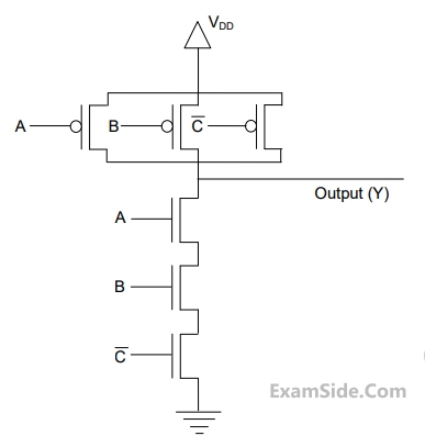
The logic function implemented by the following circuit at the terminal OUT is

GATE ECE 2008
3
The circuit diagram of a standard TTL NOT gate is shown in the figure. When $${V_i}$$= 2.5V, the modes of operation of the transistors will be:

GATE ECE 2007
4
The DTL, TTL, ECL and CMOS families of digital ICs are compared in the following 4 columns
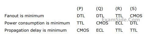
GATE ECE 2003
5
In the output stage of a standard TTL, we have a diode between the emitter of the pull up transistor and the collector of the pull-down transistor. The purpose of this diode is to isolate the output node from the power supply $${V_{cc}}$$.
GATE ECE 1994
6
Given that for a logic family,
$${V_{OH}}$$ is the minimum output high-level voltage
$${V_{OL}}$$ is the minimum output low-level voltage
$${V_{IH}}$$ is the minimum output high-level voltage and
$${V_{IL}}$$ is the minimum output low-level voltage.
The correct relationship is:
GATE ECE 1987