Semiconductor Physics · Electronic Devices and VLSI · GATE ECE

Start Practice

Marks 1

1

For non-degenerately doped n-type silicon, which one of the following plots represents the temperature ($T$) dependence of free electron concentration ($n$)?

GATE ECE 2024
2

The free electron concentration profile $n(x)$ in a doped semiconductor at equilibrium is shown in the figure, where the points A, B, and C mark three different positions. Which of the following statements is/are true?

GATE ECE 2024 Electronic Devices and VLSI - Semiconductor Physics Question 2 English
GATE ECE 2024
3

In a semiconductor, if the Fermi energy level lies in the conduction band, then the semiconductor is known as

GATE ECE 2023
4

For an intrinsic semiconductor at temperature $$T=0K$$, which of the following statement is true?

GATE ECE 2023
5

Consider a long rectangular bar of direct bandgap p-type semiconductor. The equilibrium hole density is 1017 cm$$-$$3 and the intrinsic carrier concentration is 1010 cm$$-$$3. Electron and hole diffusion lengthss are 2 $$\mu$$m and 1 $$\mu$$m, respectively. The left side of the bar (x = 0) is uniformly illuminated with a laser having photon energy greater than the bandgap of the semiconductor. Excess electron-hole pairs are generated ONLY at x = 0 because of the laser. The steady state electron density at x = 0 is 1014 cm$$-$$3 due to laser illumination. Under these conditions and ignoring electric field, the closest approximation (among the given options) of the steady state electron density at x = 2 $$\mu$$m, is _____________.

GATE ECE 2022
6

In a non-degenerate bulk semiconductor with electron density n = 1016 cm$$-$$3, the value of EC $$-$$ EFn = 200 meV, where EC and EFn denote the bottom of the conduction band energy and electron Fermi level energy, respectively. Assume thermal voltage as 26 meV and the intrinsic carrier concentration is 1010 cm$$-$$3. For n = 0.5 $$\times$$ 1016 cm$$-$$3, the closest approximation of the value of (EC $$-$$ EFn), among the given options is _________.

GATE ECE 2022
7
A bar of Gallium Arsenide (GaAs) is doped with Silicon such that the Silicon atoms occupy Gallium and Arsenic sites in the GaAs crystal. Which one of the following statement is true?
GATE ECE 2017 Set 1
8
A small percentage of impurity is added to an intrinsic semiconductor at 300 K. Which one of the following statements is true for the energy band diagram shown in the following figure? GATE ECE 2016 Set 1 Electronic Devices and VLSI - Semiconductor Physics Question 27 English
GATE ECE 2016 Set 1
9
A piece of silicon is doped uniformly with phosphorous with a doping concentration of $$10^{16}/cm^2$$. The expected value of mobility versus doping concentration for silicon assuming full dopant ionization is shown below. The charge of an electron is $$1.6\;\times\;10^{-19}\;C$$. The conductivity (in S cm-1) of the silicon sample at 300 K is _________________. GATE ECE 2015 Set 2 Electronic Devices and VLSI - Semiconductor Physics Question 28 English
GATE ECE 2015 Set 2
10
An n–type silicon sample is uniformly illuminated with light which generates 1020 electron hole pairs per cm3 per second. The minority carrier lifetime in the sample is 1 $$\mathrm\mu$$s.In the steady state, the hole concentration in the sample is approximately 10x , where x is an integer. The value of x is __________________
GATE ECE 2015 Set 2
11
A silicon sample is uniformly doped with donor type impurities with a concentration of $$10^{16}/cm^3$$.The electron and hole mobilities in the sample are $$1200\;cm^2/V-s$$ and $$400\;cm^2/V-s$$ respectively. Assume complete ionization of impurities. The charge of an electron is $$1.6\;\times\;10^{-19}\;C$$.The resistivity of the sample $$\left(in\;\Omega-cm\right)$$ is _____________.
GATE ECE 2015 Set 1
12
The cut-off wavelength (in µm) of light that can be used for intrinsic excitation of a semiconductor material of bandgap Eg= 1.1 eV is ________.
GATE ECE 2014 Set 4
13
In the figure ln(ρi) is plotted as a function of 1/T, where ρi the intrinsic resistivity of silicon, T is is the temperature, and the plot is almost linear. GATE ECE 2014 Set 4 Electronic Devices and VLSI - Semiconductor Physics Question 32 English

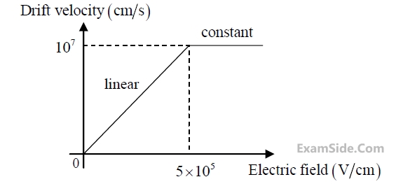
The slope of the line can be used to estimate

GATE ECE 2014 Set 4
14
A thin P-type silicon sample is uniformly illuminated with light which generates excess carriers. The recombination rate is directly proportional to
GATE ECE 2014 Set 3
15
At T = 300 K, the hole mobility of a semiconductor $$\mu_p\;=500\;cm^2/V-s$$ and $$\frac{kT}q\;=\;26\;mV$$.The hole diffusion constant Dp in cm2/s is__________.
GATE ECE 2014 Set 3
16
Drift current in the semiconductors depends upon
GATE ECE 2011
17
Which of the following is true?
GATE ECE 2008
18
Under low level injection assumption, the injected minority carrier current for an extrinsic semiconductor is essentially the
GATE ECE 2006
19
The concentration of minority carriers in an extrinsic semiconductor under equilibrium is:
GATE ECE 2006
20
The primary reason for the widespread use of Silicon in semiconductor device technology is
GATE ECE 2005
21
A Silicon PN junction at a temperature of 20°C has a reverse saturation current of 10 pico-Amperes (pA). The reverse saturation current at 40°C for the same bias is approximately
GATE ECE 2005
22
The band gap of Silicon at room temperature is:
GATE ECE 2005
23
The impurity commonly used for realizing the base region of a silicon n-p-n transistor is
GATE ECE 2004
24
n-type silicon is obtained by doping silicon with
GATE ECE 2003
25
The intrinsic carrier concentration of silicon sample at 300oK is $$1.5\times10^{16}/m^3$$. If after doping, the number of majority carriers is $$5\times10^{20}/m^3$$ , minority carrier density is
GATE ECE 2002
26
The band gap of silicon at 300 K is
GATE ECE 2002
27
The units of $$\frac q{KT}$$ are
GATE ECE 1997
28
The probability that an electron in a metal occupies the Fermi-level at any temperature (> 0 K)
GATE ECE 1995
29
In a P-type silicon sample, the hole concentration is $$2.25\times10^{15}/cm^3$$. If the intrinsic carrier concentration is $$1.5\times10^{15}/cm^3$$ , the electron concentration is
GATE ECE 1995
30
The drift velocity of electrons in silicon
GATE ECE 1995
31
A p-type silicon sample has a higher conductivity compared to an n-type sample having the same dopant concentration.
GATE ECE 1994
32
A small concentration of minority carries is injected into a homogeneous semiconductor crystal at one point. An electric field of 10 V/cm is applied across the crystal and this moves the minority carriers a distance of 1 cm is 20 $$\mu$$ sec. The mobility (in cm2/volt-sec) will be
GATE ECE 1994

Marks 2

1

A non-degenerate n-type semiconductor has 5 % neutral dopant atoms. Its Fermi level is located at 0.25 eV below the conduction band ($E_C$) and the donor energy level ($E_D$) has a degeneracy of 2. Assuming the thermal voltage to be 20 mV, the difference between $E_C$ and $E_D$ (in eV, rounded off to two decimal places) is _______.

GATE ECE 2024
2

In an extrinsic semiconductor, the hole concentration is given to be 1.5$$n_i$$ where $$n_i$$ is the intrinsic carrier concentration of 1 $$\times$$ 10$$^{10}$$ $$cm^{-3}$$. The ratio of electron to hole mobility for equal hole and electron drift current is given as ___________ (rounded off to two decimal places).

GATE ECE 2023
3

In a semiconductor device, the Fermi-energy level is 0.35 eV above the valence band energy. The effective density of states in the valence band at T = 300 K is 1 $$\times$$ 10$$^{19}$$ cm$$^{-3}$$. The thermal equilibrium hole concentration in silicon at 400 K is _____________ $$\times$$ 10$$^{13}$$ cm$$^{-3}$$ (rounded off to two decimal places).

Given kT at 300 K is 0.026 eV.

GATE ECE 2023
4

Select the CORRECT statements regarding semiconductor devices

GATE ECE 2022
5
The dependence of drift velocity of electrons on electric field in a semiconductor is shown below. The semiconductor has a uniform electron concentration of n = 1x10¹⁶ $$cm^{-3}$$ and electronic charge q = 1.6x10⁻¹⁹ C. If a bias of 5V is applied across a 1 $$\mu$$m region of this semiconductor, the resulting current density in this region, in kA/cm2, is _________. GATE ECE 2017 Set 1 Electronic Devices and VLSI - Semiconductor Physics Question 14 English
GATE ECE 2017 Set 1
6
A dc voltage of 10V is applied across an n–type silicon bar having a rectangular cross–section and a length of 1cm as shown in figure. The donor doping concentration ND and the mobility of electrons $$\mu$$n are $$10^{16}$$ cm-3 and 1000 cm2 V-1s-1, respectively. The average time (in $$\mu$$s) taken by the electrons to move from one end of the bar to other end is _______________. GATE ECE 2015 Set 2 Electronic Devices and VLSI - Semiconductor Physics Question 15 English
GATE ECE 2015 Set 2
7
Consider a silicon sample doped with ND = 1×10¹⁵/cm3 donor atoms. Assume that the intrinsic carrier concentration ni = 1.5×10¹⁰/cm3. If the sample is additionally doped with NA = 1×10¹⁸/cm3 acceptor atoms, the approximate number of electrons/cm3 in the sample, at T=300 K, will be _________________.
GATE ECE 2014 Set 4
8
An N-type semiconductor having uniform doping is biased as shown in the figure. GATE ECE 2014 Set 4 Electronic Devices and VLSI - Semiconductor Physics Question 13 English

If EC is the lowest energy level of the conduction band, EV is the highest energy level of the valance band and EF is the Fermi level, which one of the following represents the energy band diagram for the biased N-type semiconductor?

GATE ECE 2014 Set 4
9
Assume electronic charge q = 1.6×10⁻¹⁹ C, kT/q = 25 mV and electron mobility μn = 1000 cm2/V-s. If the concentration gradient of electrons injected into a P-type silicon sample is 1×10²¹/cm4, the magnitude of electron diffusion current density (in A/cm2) is _________.
GATE ECE 2014 Set 2
10
The silicon sample with unit cross-sectional area shown below is in thermal equilibrium. The following information is given: T=300K, electronic charge=1.6x10- 19C, thermal voltage=26mV and electron mobility = 1350cm2/V-s GATE ECE 2010 Electronic Devices and VLSI - Semiconductor Physics Question 18 English

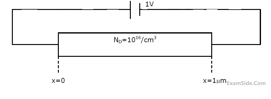
The magnitude of the electron drift current density at x=0.5 μm is

GATE ECE 2010
11
The silicon sample with unit cross-sectional area shown below is in thermal equilibrium. The following information is given: T=300K, electronic charge=1.6x10- 19C, thermal voltage=26mV and electron mobility = 1350cm2/V-s GATE ECE 2010 Electronic Devices and VLSI - Semiconductor Physics Question 19 English

The magnitude of the electric field at x=0.5 μm is

GATE ECE 2010
12
A silicon sample 'A' is doped with 1018 atoms/cm3 of Boron. Another sample 'B' of identical dimensions is doped with 1018 atoms/cm3 of Phosphorus. The ratio of electron to hole mobility is 1/3. The ratio of conductivity of the sample A to B is
GATE ECE 2005
13
An n-type silicon bar 0.1 cm long and $$100\;\mu m^2$$ in cross-sectional area has a majority carrier concentration of $$5\times10^{20}/m^3$$ and the carrier mobility is $$0.13\;\;m^2/v-s\;$$ at 300oK. if the charge of an electron is 1.6×10⁻¹⁹ coulomb, then the resistance of the bar is
GATE ECE 2003
14
The electron concentration in a sample of uniformly doped n-type silicon at 300oK varies linearly from $$10^{17}/cm^3$$ at x = 0 to $$6\times10^{16}/cm^3$$ at x = 2 $$\mu m$$. Assume a situation that electrons are supplied to keep this concentration gradient constant with time.If electronic charge is $$1.6\times10^{-19}\;coulomb$$ and the diffusion constant $$D_n=3\;cm^2/s$$, the current density in the silicon, if no electric field is present is
GATE ECE 2003
15
A semiconductor is irradiated with light such that carriers are uniformly generated throughout its volume. The semiconductor is n-type with $$N_D=10^{19}/cm^3$$. If the excess electron concentration in the steady state id $$\triangle n=10^{15}/cm^3$$ and if $$\tau_p=10\;\mu\;sec$$ [minority carrier life time] the generation rate due to irradiation
GATE ECE 1992
16
A silicon sample is uniformly doped with 1016 phosphorous atoms/cm3 and 2 ×10¹⁶ boron atoms/cm3. If all the dopants are fully ionized, the material is
GATE ECE 1991
17
In an intrinsic semiconductor the free electron concentration depends on
GATE ECE 1987
EXAM MAP
Medical
NEETAIIMS
Graduate Aptitude Test in Engineering
GATE CSEGATE ECEGATE EEGATE MEGATE CEGATE PIGATE IN
Civil Services
UPSC Civil Service
Defence
NDA
Staff Selection Commission
SSC CGL Tier I
CBSE
Class 12