FET and MOSFET · Analog Circuits · GATE ECE
Marks 1
In the circuit below, assume that the long channel NMOS transistor is biased in saturation. The small signal trans-conductance of the transistor is $g_m$. Neglect body effect, channel length modulation, and intrinsic device capacitances. The small signal input impedance $Z_{in}(j\omega)$ is _______

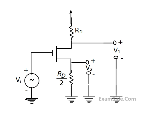
In the circuit shown below, $$V_1$$ and $$V_2$$ are bias voltages. Based on input and output impedances, the circuit behaves as a

Consider the CMOS circuit shown in the figure (substrates are connected to their respective sources). The gate width (W) to gate length (L) ratios $$\left( {{W \over L}} \right)$$ of the transistors are as shown. Both the transistors have the same gate oxide capacitance per unit area. For the pMOSFET, the threshold voltage is $$-$$1 V and the mobility of holes is $$40{{c{m^2}} \over {V.s}}$$. For the nMOSFET, the threshold voltage is 1 V and the mobility of electrons is $$300{{c{m^2}} \over {V.s}}$$. The steady state output voltage V0 is ___________.

The ideal long channel nMOSFET and pMOSFET devices shown in the circuits have threshold voltages of 1 V and $$-$$1 V, respectively. The MOSFET substrates are connected to their respectively sources. Ignore leakage currents and assume that the capacitors are initially discharged. For the applied voltages as shown, the steady state voltages are ____________.

For the transistor $M_1$ in the circuit shown in the figure, $\mu_n C_{o x}=100 \mu \mathrm{~A} / V^2$ and $\frac{W}{L}=10$, where $\mu_n$ is the mobility of electron, $C_{o x}$ is the oxide capacitance per unit area. $W$ is the width and $L$ is the length.
 The channel length modulation coefficient is ignored. If the gate-to-source voltage $V_{G S}$ is 1 V to keep the transistor at the edge of saturation. Then the threshold voltage of the transistor (rounded off to one decimal place) is $\_\_\_\_$ V.
In the circuit shown in the figure, the transistors $M_1$ and $M_2$ are operating in saturation. The channel length
modulation coefficients of both the transistors are non-zero. The transconductance of the MOSFETs $M_1$ and $M_2$ are $g_{m 1}$ and $g_{m 2}$, respectively, and the internal resistance of the MOSFETs $M_1$ and $M_2$ are $r_{01}$ and $r_{02}$ respectively.
 Ignoring the body effect, the ac small signal voltage gain ( $d V_{\text {out }} / d V_{\text {in }}$ ) of the circuit is
Marks 2
An $n$-channel MOSFET is connected as shown in the Figure.
Assume $\mathrm{V}_{\mathrm{TH}}=1 \mathrm{~V}, V_{D D}=5 \mathrm{~V}$, and $\mu C_{O x}\left(\frac{W}{L}\right)=2 \mathrm{mAV}^{-2}$ and neglect channel length modulation effects.
The gate voltage ( $V_G$ ) of the n-channel MOSFET (in Volt) is $\_\_\_\_$ . (rounded off to two decimal places)

The identical MOSFETs $M_1$ and $M_2$ in the circuit given below are ideal and biased in the saturation region. $M_1$ and $M_2$ have a transconductance $g_m$ of 5 mS .
The input signals (in Volts) are:
$$ \begin{aligned} & V_1=2.5+0.01 \sin \omega t \\ & V_2=2.5-0.01 \sin \omega t \end{aligned} $$
The output signal $V_3$ (in Volts) is _ .

In the circuit shown below, the transistors $M_1$ and $M_2$ are biased in saturation. Their small signal transconductances are $g_{m1}$ and $g_{m2}$ respectively. Neglect body effect, channel length modulation and intrinsic device capacitances.

Assuming that capacitor $C_i$ is a short circuit for AC analysis, the exact magnitude of small signal voltage gain $\left| \frac{v_{out}}{v_{in}} \right|$ is ______.
An NMOS transistor operating in the linear region has $I_{D}$ of 5 $\mu$A at $V_{DS}$ of 0.1 V. Keeping $V_{GS}$ constant, the $V_{DS}$ is increased to 1.5 V.
Given that $\mu_{n}C_{ox} \frac{W}{L}$ = 50 $\mu$A/$V^2$, the transconductance at the new operating point (in $\mu$A/V, rounded off to two decimal places) is ______.
Consider an ideal long channel nMOSFET (enhancement-mode) with gate length 10 $$\mu$$m and width 100 $$\mu$$m. The product of electron mobility ($$\mu$$n) and oxide capacitance per unit area (Cox) is $$\mu$$nCox = 1 mA/V2. The threshold voltage of the transistor is 1 V. For a gate-to-source voltage VGS = [2 $$-$$ sin(2t)] V and drain-to source voltage VDS = 1 V (substrate connected to the source), the maximum value of the drain-to-source current is ___________.
Consider the circuit shown with an ideal long channel nMOSFET (enhancement mode, substrate is connected to the source). The transistor is appropriately biased in the saturation region with VGG and VDD such that it acts as a linear amplifier. vi is the small-signal ac input voltage. vA and vB represent the small-signal voltages at the nodes A and B, respectively. The value of $${{{v_A}} \over {{v_B}}}$$ is __________ (rounded off to one decimal place).

For an $n$-channel silicon MOSFET with 10 nm gate oxide thickness, the substrate sensitivity ( $\partial V_T / \partial\left|V_{B S}\right|$ ) is found to be $50 \mathrm{mV} / \mathrm{V}$ at a substrate voltage $\left|V_{B S}\right|=2 \mathrm{~V}$, where $V_T$ is the threshold voltage of the MOSFET. Assume that, $\left|V_{B S}\right| \gg 2 \phi_B$, where $q \phi_B$ is the separation between the Femi energy level $E_F$ and the intrinsic level $E_i$ in the bulk. Parameters given are
Electron charge $(q)=1.6 \times 10^{-9} \mathrm{C}$
Vacuum permittivity $\left(\varepsilon_o\right)=8.85 \times 10^{-12} \mathrm{~F} / \mathrm{m}$
Relative permittivity of silicon $\left(\varepsilon_{S i}\right)=12$
Relative permittivity of oxide $\left(\varepsilon_{o x}\right)=4$
The doping concentration of the substrate is
Using the incremental low frequency small - signal model of the MOS device, the Norton equivalent resistance of the following circuit is

An enhancement MOSFET of threshold voltage 3 V is being used in the sample and hold circuit given below. Assume that the substrate of the MOS device is connected to -10 V . If the input voltage $v_1$ liesbetween $\pm 10 \mathrm{~V}$, the minimum and the maximum value of $v_G$ required for proper sampling and holding respectively, are


(i)VGS = 0 at Id = 12 mA and
(ii)VGS = -6 Volts at Zo =$$\infty $$
Which of the following Q-points will give the highest transconductance gain for small signals?
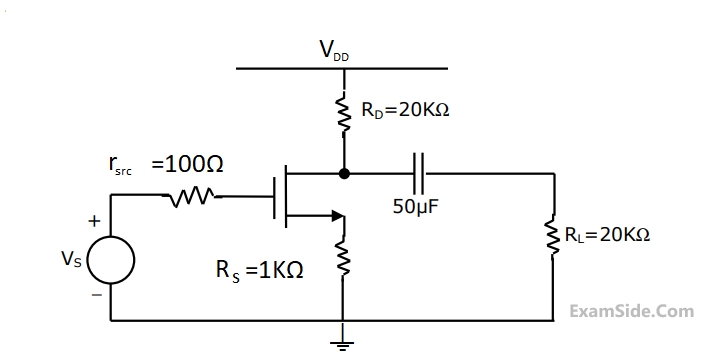
$${r_d} = 20K\Omega ,\,\,{I_{DSS}}\, = \,10mA,\,\,{V_P} = - 8V$$

Zi and Zo of the circuit are respectively
$${r_d} = 20K\Omega ,\,\,{I_{DSS}}\, = \,10mA,\,\,{V_P} = - 8V$$
Transconductance in milli-Siemens (mS) and voltage gain of the amplifier are respectively.
$${r_d} = 20K\Omega ,\,\,{I_{DSS}}\, = \,10mA,\,\,{V_P} = - 8V$$
ID and VDS under DC conditions are respectively


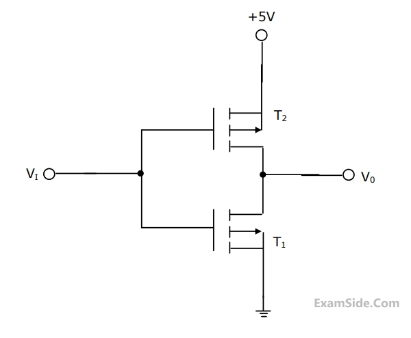
Statement 1: T1 conducts when Vi $$ \ge \,2\,V$$.
Statement 2: T1 is always in saturation when $${V_0}\, = \,0\,V$$.
Which of the following is correct?

Marks 5