BJT and FET · Electronic Devices and VLSI · GATE ECE
Marks 1
1
Figure shows the output characteristics of two different Bipolar Junction
Transistors (BJT), BJT 1 with magnitude of Early voltage $\left|V_{A 1}\right|$, and BJT 2 with magnitude of Early voltage $\left|V_{A 2}\right|$.
Which of the following options is/are correct regarding the Early voltages?

GATE ECE 2026
2
An ideal MOS capacitor (p-type semiconductor) is shown in the figure. The MOS capacitor is under strong inversion with VG = 2V. The corresponding inversion charge density (QIN) is 2.2 $$\mu$$C/cm2. Assume oxide capacitance per unit area as Cox = 1.7 $$\mu$$F/cm2. For VG = 4V, the value of QIN is __________ $$\mu$$C/cm2 (rounded off to one decimal place).

GATE ECE 2022
3
For a narrow base PNP BJT, the excess minority carrier concentration ($$\bigtriangleup n_E$$ for emitter,
$$\bigtriangleup p_B$$ for base, $$\bigtriangleup n_E$$ for collector) normalized to equilibrium minority carrier concentration
($$\bigtriangleup n_{E0}$$ for emitter, $$\bigtriangleup p_{B0}$$ for base, $$\bigtriangleup n_{C0}$$ for collector) in the quasi-neutral emitter, base and collector
regions are shown below. Which one of the following biasing modes is the transistor operating in?
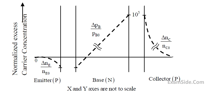
GATE ECE 2017 Set 1
4
Consider the circuit shown in the figure. Assume base-to-emitter voltage VBE=0.8 V and common base current gain $$\left(\alpha\right)$$ of the transistor is unity.
 The value of the collector-to–emitter voltage VCE (in volt) is _______.
The value of the collector-to–emitter voltage VCE (in volt) is _______.GATE ECE 2017 Set 2
5
An npn bipolar junction transistor (BJT) is operating in the active region. If the reverse bias
across the base-collector junction is increased, then
GATE ECE 2017 Set 2
6
The Ebers-Moll model of a BJT is valid
GATE ECE 2016 Set 2
7
The figure shows the I-V characteristics of a solar cell illuminated uniformly with solar light of
power 100 mW/cm2. The solar cell has an area of 3 cm2 and a fill factor of 0.7. The maximum efficiency (in %) of the device is __________.

GATE ECE 2016 Set 3
8
If the base width in a bipolar junction transistor is doubled, which one of the following
statements will be TRUE?
GATE ECE 2015 Set 3
9
In the circuit shown in the figure, the BJT has a current gain (β) of 50. For an emitter-base
voltage VEB = 600 mV, the emitter-collector voltage VEC(in Volts) is ______.
GATE ECE 2015 Set 3
10
An increase in the base recombination of a BJT will increase
GATE ECE 2014 Set 2
11
For a BJT the common base current gain $$\alpha$$ = 0.98 and the collector base junction
reverse bias saturation current ICO = 0.6μA. This BJT is connected in the common
emitter mode and operated in the active region with a base drive current
IB=20μA. The collector current IC for this mode of operation is
GATE ECE 2011
12
If the transistor in Figure is in saturation, then
GATE ECE 2002
13
MOSFET can be used as a
GATE ECE 2001
14
A BJT is said to be operating in the saturation region if
GATE ECE 1995
15
The Ebers-Moll model is applicable to
GATE ECE 1995
16
The Early-Effect in a bipolar junction transistor is caused by
GATE ECE 1995
17
The breakdown voltage of a transistor with its base open is
BVCEO with
emitter open is BVCBO, then
GATE ECE 1995
18
Channel current is reduced on application of a more positive voltage to the gate
of a depletion mode n-channel MOSFET.
GATE ECE 1994
19
The transit time of the current carriers through the channel of an FET decides
its ____________characteristics.
GATE ECE 1994
Marks 2
1
The injected excess electron concentration profile in the base region of an npn BJT, biased in the
active region, is linear, as shown in the figure. If the area of the emitter-base junction is 0.001 cm2, µn = 800 cm2/(V-s) in the base region and depletion layer widths are negligible, then the collector
current Ic (in mA) at room temperature is __________.
(Given: thermal voltage VT = 26 mV at room temperature, electronic charge q = $$1.6\times10^{-19}\;C$$ )

GATE ECE 2016 Set 3
2
An npn BJT having reverse saturation current $$I_s\;=\;10^{-15}\;A$$ is biased in the forward active
region with VBE = 700 mV. The thermal voltage (VT) is 25 mV and the current gain (β)
may vary from 50 to 150 due to manufacturing variations. The maximum emitter current
(in μA) is _____.
GATE ECE 2015 Set 3
3
Consider two BJT's biased at the same collector current with area A1 = 0.2 μm × 0.2 μm and
A2 = 300 μm × 300 μm. Assuming that all other device parameters are identical, kT/q = 26
mV, the intrinsic carrier concentration is 1 × 1010 cm-3, and q = 1.6 × 10⁻¹⁹ C, the difference
between the base-emitter voltages (in mV) of the two BJT's (i.e., VBE1 – VBE2) is___________.
GATE ECE 2014 Set 4
4
The channel resistance of an N-channel JFET shown in the figure below is 600 W
when the full channel thickness (tch) of 10 μm is available for conduction. The
built-in voltage of the gate P+N junction (Vbi) is -1 V. When the gate to source
voltage (VGS) is 0 V, the channel is depleted by 1 μm on each side due to the built in
voltage and hence the thickness available for conduction is only 8 μm
 The channel resistance when VGS = 0 V is
The channel resistance when VGS = 0 V isGATE ECE 2011
5
The channel resistance of an N-channel JFET shown in the figure below is 600 W
when the full channel thickness (tch) of 10 μm is available for conduction. The
built-in voltage of the gate P+N junction (Vbi) is -1 V. When the gate to source
voltage (VGS) is 0 V, the channel is depleted by 1 μm on each side due to the built in
voltage and hence the thickness available for conduction is only 8 μm
The channel resistance when VGS = -3 V is
The channel resistance when VGS = -3 V isGATE ECE 2011
6
In a uniformly doped BJT, assume that NE, NB and NC are the emitter, base and
collector dopings in atoms/cm3, respectively. If the emitter injection efficiency of
the BJT is close unity, which one of the following conditions is TRUE?
GATE ECE 2010
7
The DC current gain ($$\beta$$) of a BJT is 50. Assuming that the emitter injection
efficiency is 0.995, the base transport factor is:
GATE ECE 2007
8
An n-channel JEFT has IDSS = 2 mA and Vp = −4 V. It's transconductance gm (in
mA/V) for an applied gate-to-source voltage VGS of –2V is:
GATE ECE 1999
9
An n-channel JFET has a pinch-off voltage VP = -5 V, VDS(max) = 20 V and gm = 2 mA/V. The minimum ‘ON’ resistance is achieved in the JEFT for
GATE ECE 1992
10
In a transistor having finite B, the forward bias across the base emitter junction
is kept constant and the reverse bias across the collector base junction is
increased. Neglecting the leakage across the collector base junction and the
depletion region generating current, the base current will __________.
(increase/decrease/remain constant).
GATE ECE 1992