PN Junction · Electronic Devices and VLSI · GATE ECE
Marks 1
Consider carrier transport in a Zener diode in the breakdown region. Which is the dominant transport mechanism for current flow in this case?
Consider a p-n junction diode when it is forward biased with 2 V . Which of the following is/are the correct magnitude(s) of the energy difference between quasi Fermi-levels, $E_{f n}$ in the n -side and $E_{f p}$ in the $p$-side?
A silicon $P-N$ junction is shown in the figure. The doping in the $P$ region is $5 \times 10^{16} \mathrm{~cm}^3$ and doping in the $N$ region is $10 \times 10^{-16} \mathrm{~cm}^{-3}$. The parameters given are
Built-in voltage $\left(\phi_{b i}\right)=0.8 \mathrm{~V}$
Electro charge $(q)=1.6 \times 10^{-19} \mathrm{C}$
Vacuum permittivity of silicon $\left(\varepsilon_{s i}\right)=12$
 The magnitude of reverse bias voltage that would completely deplete one of the two regions ( $P$ or $N$ ) prior to the other (rounded off to one decimal place) is $\_\_\_\_$ V.
Consider the recombination process via bulk traps in a forward biased $p n$ homojunction diode. The maximum recombination rate is $U_{\max }$. If the electron and the hole capture cross sections are equal, which one of the following is FALSE?


The maximum and minimum values of the output voltage respectively are
Marks 2
Consider an LED based on a direct bandgap semiconductor material with energy bandgap 1.3 eV .
Given: Plank's constant, $h=6.63 \times 10^{-34} \mathrm{~J} \mathrm{~s}$ and speed of light in free space is $3 \times 10^8 \mathrm{~m} \mathrm{~s}^{-1}$.
In which of the following wavelength ranges the LED will NOT emit?
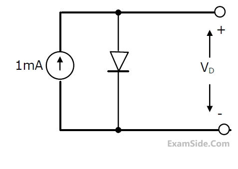
The photocurrent of a PN junction diode solar cell is 1 mA. The voltage corresponding to its maximum power point is 0.3 V. If the thermal voltage is 30 mV, the reverse saturation current of the diode (in nA, rounded off to two decimal places) is _____.
A p-type semiconductor with zero electric field is under illumination (low level injection) in steady state condition. Excess minority carrier density is zero at x = $$\pm$$ 2ln, where ln = 10$$-$$4 cm is the diffusion length of electrons. Assume electronic charge, q = $$-$$1.6 $$\times$$ 10$$-$$19 C. The profiles of photo-generation rate of carriers and the recombination rate of excess minority carriers (R) are shown. Under these conditions, the magnitude of the current density due to the photo-generated electrons at x = +2ln is ___________ mA/cm2 (rounded off to two decimal places).

A $p n$ junction solar cell of area $1.0 \mathrm{~cm}^2$, illuminated uniformly with $100 \mathrm{mWcm}^{-2}$; has the following parameter : Efficiency $=15 \%$, open circuit voltage $=0.7 \mathrm{~V}$, fill factor $=0.8$, and thickness $=200 \mu \mathrm{~m}$. The charge of an electron is $1.6 \times 10^{-19} \mathrm{C}$. The average optical generation rate ( $\mathrm{in} \mathrm{cm}^{-3} \mathrm{~s}^{-1}$ ) is
A one-sided abrupt $p n$ junction diode has a depletion capacitance $C_D$ of 50 pF at a reverse bias 0.2 V . The plot of $\frac{1}{C_D^2}$ versus the applied voltage $V$ for this diode is a straight line as shown in the figure below. The slope of the plot is $\_\_\_\_$ $\times 10^{20} \mathrm{~F}^{-2} \mathrm{~V}^{-1}$.


Given q = 1.6 × 10⁻¹⁹ coulomb, $$\varepsilon$$0 = 8.85 × 10⁻¹⁴ F/cm, $$\varepsilon$$r = 11.7 for silicon, the value of L in nm is ________.


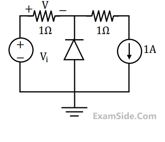


(Give the sketch showing the magnitudes of the current at t = 0, t = t0 and t = $$\infty$$ )
