Addressing of a $32 K \times 16$ memory is realized using a single decoder. The minimum number of AND gates required for the decoder is :
A
$2^{19}$
B
$2^8$
C
$2^{32}$
D
$2^{15}$
2
GATE ECE 2018
MCQ (Single Correct Answer)
+2
-0.67
A 2 $$ \times $$ 2 ROM array is built with the help of diodes as shown in the circuit below. Here W0
and W1 are signals that select the word lines and B0 and B1 are signals that are output of the
sense amps based on the stored data corresponding to the bit lines during the read operation.
During the read operation, the selected word line goes high and the other word line is in a
high impedance state. As per the implementation shown in the circuit diagram above, what
are the bits corresponding to Dij (where i = 0 or 1 and j = 0 or 1) stored in the ROM?
If WL is the Word Line and BL the Bit Line, an SRAM cell is shown in
A
B
C
D
4
GATE ECE 2003
MCQ (Single Correct Answer)
+2
-0.6
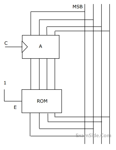
In the circuit shown in Figure, A is a parallel in, parallel-out 4-bit register, which loads at the rising edge of the clock C. The input lines are connected to a 4-bit bus, W. Its output acts as the input to a 16×4 ROM whose output is floating when
the enable input E is 0. A partial table of the contents of the ROM is as follows
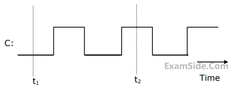
The clock to the register is shown, and the data on the W bus at time t$$_1$$ is 0110. The data on the bus at time t$$_2$$ is