Combinational Circuits · Digital Circuits · GATE ECE
Marks 1
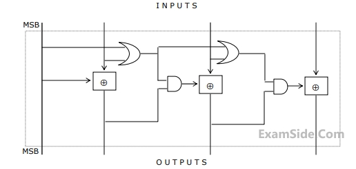
A full adder and an XOR gate are used to design a digital circuit with inputs $X, Y$, and $Z$, and output $F$, as shown below. The input $Z$ is connected to the carry-in input of the full adder.
If the input $Z$ is set to logic ' 1 ', then the circuit functions as __________ with $X$ and $Y$ as inputs.

In the circuit shown below, P and Q are the inputs. The logical function realized by the circuit shown below is

Consider the 2-bit multiplexer (MUX) shown in the figure. For OUTPUT to be the XOR of C and D, the values for A0, A1, A2 and A3 are ___________.

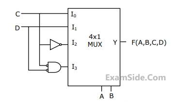
The propagation delays of the XOR gate, AND gate and multiplexer (MUX) in the circuit shown in the figure are $4 \mathrm{~ns}, 2 \mathrm{~ns}$ and 1 ns respectively.
 If all the inputs $P, Q, R, S$ and $T$ are applied simultaneously and held constant, the maximum propagation delay of the circuit is
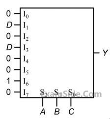
The figure below shows a multiplexer where $S_1$ and $S_0$ are the select lines, $I_0$ to $I_3$ are the input data lines, $E N$ is the enable line, and $F(P, Q, R)$ is the output. $F$ is

 The Boolean expression F implemented by the circuit is
 Which one of the following statements correctly describes the choice of signals to be connected to the inputs $${I_0}$$, $${I_1}$$, $${I_2 }$$ and $${I_3}$$ so that the output is C$$_{out}$$?


Marks 2
A Boolean function, $f(x, y, z)$ with $x$ as MSB and $z$ as LSB is realized by $4: 1$ multiplexer (MUX) with select lines, $S_1$ and $S_0$ ( $S_1$ is MSB, $S_0$ is LSB) and inputs, $I_0, I_1, I_2, I_3$ as shown in the Figure.
Which of the following options is the correct expression of $f(x, y, z)$ ?

A 4-bit priority encoder has inputs $D_3, D_2, D_1,$ and $D_0$ in descending order of priority. The two-bit output $AB$ is generated as 00, 01, 10, and 11 corresponding to inputs $D_3, D_2, D_1,$ and $D_0$, respectively. The Boolean expression of the output bit $B$ is _______.
The propagation delay of the 2 x 1 MUX shown in the circuit is 10 ns. Consider the propagation delay of the inverter as 0 ns.

If S is set to 1 then the output Y is _______.

The minimized expression for F(U, V, W, X) is
 The Boolean function F implemented is
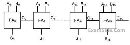
 At t=0, the inputs to the 4-bit adder are changed to $${X_3}$$$${X_2}$$$${X_1}$$$${X_0}$$ =1100, $${Y_3}$$$${Y_2}$$$${Y_1}$$$${Y_0}$$ = 0100 and $${Z_0}$$=1.
The output of the ripple carry adder will be stable at t (in ns) = ____
At t=0, the inputs to the 4-bit adder are changed to $${X_3}$$$${X_2}$$$${X_1}$$$${X_0}$$ =1100, $${Y_3}$$$${Y_2}$$$${Y_1}$$$${Y_0}$$ = 0100 and $${Z_0}$$=1.
The output of the ripple carry adder will be stable at t (in ns) = ____


Y = $$\,P \oplus \,Q\, \oplus \,R$$
z= $$RQ + \overline P R\, + Q\,\overline P $$
 The circuit acts as a

Marks 5
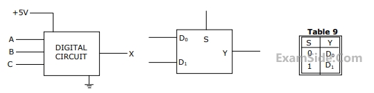 ( $$\overline A \,\overline B \,and\,\overline {C\,} $$ and are not available). The +5V power supply (logic 1) and the ground
(logic 0) are also available. The output of the circuit is X = $$\overline A \,B + \,\overline A \,\overline B \,\,\overline {C\,} $$
( $$\overline A \,\overline B \,and\,\overline {C\,} $$ and are not available). The +5V power supply (logic 1) and the ground
(logic 0) are also available. The output of the circuit is X = $$\overline A \,B + \,\overline A \,\overline B \,\,\overline {C\,} $$
Marks 8

Marks 10
$${F_1}$$$$(A,\,B,\,C,\,D) = ABCD + \bar A\,\overline B \,\bar C\,\bar D$$
$${F_2}(A,\,B,\,C,\,D) = (A + B)(\bar A\, + \overline B + C)$$
$${F_3}(A,\,B,\,C,\,D) = \sum {13,15 + \sum {3,5} } $$
(a) What is the minimum size of the ROM required?
(b) Determine the data in each location of the ROM.
(1) What will be the minimized SOP expression for F?
(2) Implement this function on an 8 : 1 MUX.
$$f(A,B,C,D) = B.C + A.B.\bar D + \bar A.\bar C.\bar D$$
(1) Pressure (P) is low or high'
(2) Temperature (T) is low or high' and
(3) Liquid level (L) is low or high.
its has two controls - Heater (H) which is either on or off and inlet value (V) which is open or close. The controls are operated as per Table.
(a) Using the convertion High =1, Low = 0, On=1, Off=0, Open=1 and Closed=0, draw the Karnaugh maps for H and V.
(b) Obtain the minimal product of sums expressions for H and V.
(c) Realize the logic for H and V using two 4-input multiplexers with T and L as control inputs. Used T as MSB.
