1
GATE ECE 2013
MCQ (Single Correct Answer)
+2
-0.6
In the circuit shown below, Q1 has negligible collector-to-emitter saturation voltage and the diode
drops negligible voltage across it under forward bias. If VCC is +5 V, X and Y are digital signals
with 0 V as logic 0 and VCC as logic 1, then the Boolean expression for Z is

2
GATE ECE 2008
MCQ (Single Correct Answer)
+2
-0.6
The logic function implemented by the following circuit at the terminal OUT is

3
GATE ECE 2007
MCQ (Single Correct Answer)
+2
-0.6
The circuit diagram of a standard TTL NOT gate is shown in the figure. When $${V_i}$$= 2.5V, the modes of operation of the transistors will be:

4
GATE ECE 2003
MCQ (Single Correct Answer)
+2
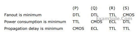
-0.6
The DTL, TTL, ECL and CMOS families of digital ICs are compared in the following 4 columns
GATE ECE Subjects
Browse all chapters by subject
Control Systems
Engineering Mathematics
Analog Circuits
Network Theory
Electromagnetics
Electronic Devices and VLSI
Digital Circuits
Microprocessors
Signals and Systems
Discrete Fourier Transform and Fast Fourier Transform Discrete Time Signal Fourier Series Fourier Transform Continuous Time Signal Laplace Transform Fourier Transform Representation of Continuous Time Signal Fourier Series Transmission of Signal Through Continuous Time LTI Systems Miscellaneous Sampling Continuous Time Linear Invariant System Discrete Time Linear Time Invariant Systems Discrete Time Signal Z Transform Transmission of Signal Through Discrete Time Lti Systems
Communications
General Aptitude