Analog to Digital and Digital to Analog Converters · Digital Circuits · GATE ECE

Start Practice

Marks 1

1
A 4-bit weighted-resistor DAC with inputs $b_3, b_2, b_1$, and $b_0$ (MSB to LSB) is designed using an ideal opamp, as shown below. The switches are closed when the corresponding input bits are logic ' 1 ' and open otherwise. When the input $b_3 b_2 b_1 b_0$ changes from 1110 to 1101, the magnitude of the change in the output voltage $V_O$ (in mV , rounded off to the nearest integer) is ____________. GATE ECE 2025 Digital Circuits - Analog to Digital and Digital to Analog Converters Question 1 English
GATE ECE 2025
2

The signal-to-noise ratio (SNR) of an ADC with a full-scale sinusoidal input is given to be 61.96 dB. The resolution of the ADC is __________ bits (rounded off to the nearest integer).

GATE ECE 2023
3
Consider a four bit D to A converter. The analog value corresponding to digital signals of values 0000 and 0001 are 0 V and 0.0625 V respectively. The analog value (in Volts ) corresponding to the digitals signal 1111 is ______________.
GATE ECE 2015 Set 1
4
The number of comparators required in a 3-bit comparator type ADC is
GATE ECE 2002
5
The number of comparators in 4-bit flash ADC is
GATE ECE 2000
6
The resolution of a 4-bit counting ADC is 0.5 Volts. For an analog input of 6.6 Volts, the digital output of the ADC will be
GATE ECE 1999
7
The advantage of using a dual slope ADC in a digital voltmeter is that
GATE ECE 1998
8
For an ADC, match the following : if
List 1
A. Flash converter
B. Dual slope converter
C. Successive approximation Converter

List 2
1. requires a conversion time of the order of a few seconds
2. requires a digital- to- analog converter
3. minimizes the effect of power supply interference.
4. requires a very complex hardware.
5. It is a tracking A/D converter.
GATE ECE 1998
9
A 12-bit ADC is operating with a 1$$\mu $$ sec clock period and the total conversion time is seen to be 14 $$\mu $$ sec. The ADC must br of the
GATE ECE 1996
10
Match the List-1 (type of 8-bit ADC) with List-2(Minimum conversion time in clock cycles)

List - 1


A. Successive approximation
B. Dual-slope
C. Parallel Comparator

List - 2


1) 1
2) 8
3) 16
4) 256
5) 512
GATE ECE 1994
11
Which of the resistance networks of figure can be used as 3 bit R-2R ladder DAC. Assume $${V_0}$$ corresponds to LSB. GATE ECE 1990 Digital Circuits - Analog to Digital and Digital to Analog Converters Question 12 English 1 GATE ECE 1990 Digital Circuits - Analog to Digital and Digital to Analog Converters Question 12 English 2 GATE ECE 1990 Digital Circuits - Analog to Digital and Digital to Analog Converters Question 12 English 3
GATE ECE 1990

Marks 2

1
A 10-bit analog-to-digital converter (ADC) has a sampling frequency of 1 MHz and a full scale voltage of 3.3 V . For an input sinusoidal signal with frequency 500 kHz , the maximum SNR (in dB, rounded off to two decimal places) and the data rate (in Mbps) at the output of the ADC are _________ , respectively.
GATE ECE 2025
2

A full scale sinusoidal signal is applied to a 10-bit ADC. The fundamental signal component in the ADC output has a normalized power of 1 W, and the total noise and distortion normalized power is 10 $\mu$W. The effective number of bits (rounded off to the nearest integer) of the ADC is _______.

GATE ECE 2024
3

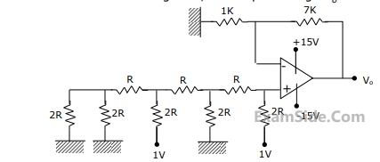
Consider the circuit shown with an ideal OPAMP. The output voltage V0 is __________ V (rounded off to two decimal places).

GATE ECE 2022 Digital Circuits - Analog to Digital and Digital to Analog Converters Question 5 English

GATE ECE 2022
4
In an N bit flash ADC, the analog voltage is fed simultaneously to 2N− 1 comparators. The output of the comparators is then encoded to a binary format using digital circuits. Assume that the analog voltage source Vin(whose output is being converted to digital format) has a source resistance of 75 Ω as shown in the circuit diagram below and the input capacitance of each comparator is 8 pF. The input must settle to an accuracy of 1/2 LSB even for a full scale input change for properconversion. Assume that the time taken by the thermometer to binary encoder is negligible. GATE ECE 2016 Set 2 Digital Circuits - Analog to Digital and Digital to Analog Converters Question 11 English If the flash ADC has 8 bit resolution, which one of the following alternatives is closest to the maximum sampling rate?
GATE ECE 2016 Set 2
5
In the following circuit, the comparator output is logic “I” if V1 > V2 and is logic “0” otherwise. The D/A conversion is done as per the relation $$${V_{DAC}} = \sum\limits_{n = 0}^3 {{2^{n - 1}}{b_n}\,\,} Volts,$$$ where b3(MSB), b2, b1 and b0 (LSB) are the counter outputs.

The counter starts from the clear state.

GATE ECE 2008 Digital Circuits - Analog to Digital and Digital to Analog Converters Question 7 English

The stable reading of the LED display is

GATE ECE 2008
6
In the following circuit, the comparator output is logic “I” if V1 > V2 and is logic “0” otherwise. The D/A conversion is done as per the relation $$${V_{DAC}} = \sum\limits_{n = 0}^3 {{2^{n - 1}}{b_n}\,\,} Volts,$$$ where b3(MSB), b2, b1 and b0 (LSB) are the counter outputs.

The counter starts from the clear state.

GATE ECE 2008 Digital Circuits - Analog to Digital and Digital to Analog Converters Question 6 English

The magnitude of the error between VDAC and Vin at steady state in volts is

GATE ECE 2008
7
In the digital-to-Analog converter circuit shown in the figure below,
$${V_{R\,}}\, = \,10V$$ and $$R\, = \,10k\Omega $$ GATE ECE 2007 Digital Circuits - Analog to Digital and Digital to Analog Converters Question 9 English

The current i is

GATE ECE 2007
8
In the digital-to-Analog converter circuit shown in the figure below,
$${V_{R\,}}\, = \,10V$$ and $$R\, = \,10k\Omega $$ GATE ECE 2007 Digital Circuits - Analog to Digital and Digital to Analog Converters Question 8 English

The voltage V0 is

GATE ECE 2007
9
A 4-bit D/A converter is connected to a free-running 3-bit UP counter, as shown in the following figure. Which of the following waveforms will be observed at V0=? GATE ECE 2006 Digital Circuits - Analog to Digital and Digital to Analog Converters Question 10 English

In the figure shown above, the ground has been shown by the symbol $$\nabla $$

GATE ECE 2006
10
The circuit shown in figure is a 4-bit DAC GATE ECE 2003 Digital Circuits - Analog to Digital and Digital to Analog Converters Question 14 English The input bits 0 and 1 are represented by 0 and 5 V respectively. The OP- AMP is ideal, but all the resistances and the 5V inputs have a tolerance of ±10%.
The specification (rounded to the nearest multiple of 5%) for the tolerance of the DAC is
GATE ECE 2003
11
For the 4 bit DAC shown in Figure, the output voltage $${V_0}$$ is GATE ECE 2000 Digital Circuits - Analog to Digital and Digital to Analog Converters Question 15 English
GATE ECE 2000
EXAM MAP
Medical
NEETAIIMS
Graduate Aptitude Test in Engineering
GATE CSEGATE ECEGATE EEGATE MEGATE CEGATE PIGATE IN
Civil Services
UPSC Civil Service
Defence
NDA
Staff Selection Commission
SSC CGL Tier I
CBSE
Class 12