Logic Gates · Digital Circuits · GATE ECE
Marks 1
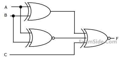
In the circuit shown in the Figure, $A$ and $B$ are logic inputs and $Y$ is the logic output. Which of the following logic operations is realized by the circuit?

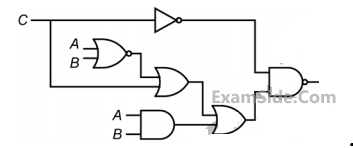
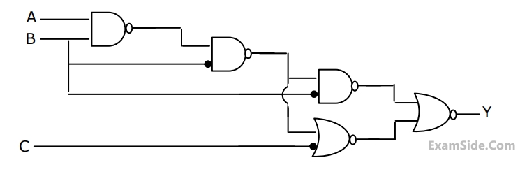
For the circuit shown below, the propagation delay of each NAND gate is 1 ns. The critical path delay, in ns, is __________ (rounded off to the nearest integer).


Marks 2
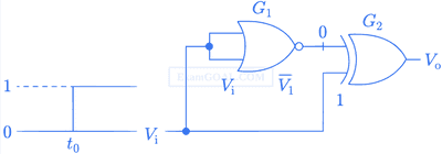
Consider a Boolean gate (D) where the output Y is related to the inputs A and b as, Y = A + $$\overline B $$, where + denotes logical OR operation. The Boolean inputs '0' and '1' are also available separately. Using instances of only D gates and inputs '0' and '1', ___________ (select the correct options).

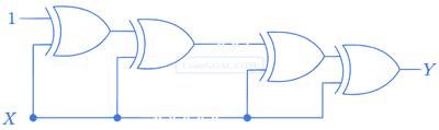
The number of distinct values of X3X2X1X0 (out of the 16 possible values) that give 𝑌 = 1 is _______.


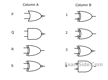
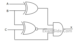
Which one of the following statesments is TRUE?


Marks 5


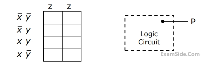
(a) Enter the logical values in the given Karnaugh map [figure2(b)] for the output
Y.
(b) Write down the expression for Y in sum-of products from using minimum
number of terms.
(c) Draw the circuit for the digital logic boxes using four 2-input NAND gates
only for each of the boxes.
(a) Enter the logical values in the K-map in the format shown in figure 3(a). Derive
the minimal Boolean sum-of-products expression whose output is zero when a majority of the pumps fail.
(b) The above expression is implemented using logic gates, and point P is the
output of this circuit, as shown in figure 3(b). P is at 0 V when a majority of the pumps fails and is at 5 V otherwise. Design a circuit to drive the LED using this output. The current through the LED should be 10 mA and the voltage drop across it is 1V. Assume that P can source or sink 10 mA and a 5 V supply is available.
