Bipolar Junction Transistor · Analog Circuits · GATE ECE
Marks 1
A simplified small-signal equivalent circuit of a BJT-based amplifier is given below. The small-signal voltage gain $V_o / V_s$ (in $\mathrm{V} / \mathrm{V}$ ) is_________.


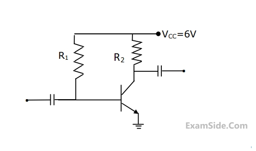
The value of R2 (in $$\Omega $$ ) for which I2 = 100 $$\mu {\rm A}$$ is ________.

A1: Av0 = 10,Rin = 10 kΩ ,R0 =1 kΩ
A2 : Av0 = 5,Rin = 5 kΩ , R0 = 200 Ω
The approximate overall voltage gain $$\frac{{\mathrm V}_\mathrm{out}}{{\mathrm V}_\mathrm{in}}$$ is ______.

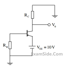


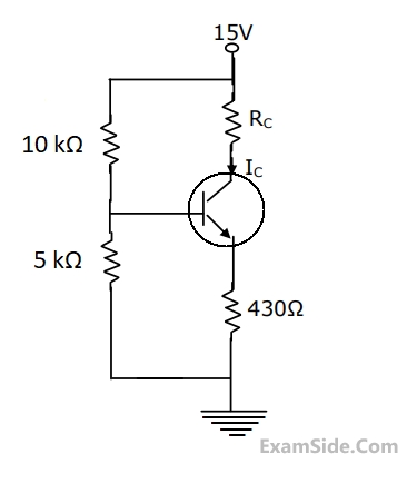
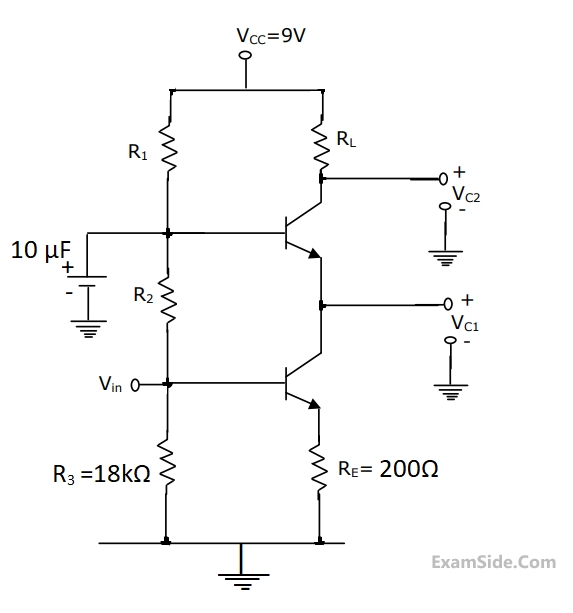
A transistor having $$\alpha$$ = 0.99 and VBE = 0.7 V, is used in the circuit of the figure.What is the value of the collector current?


Marks 2
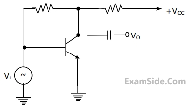
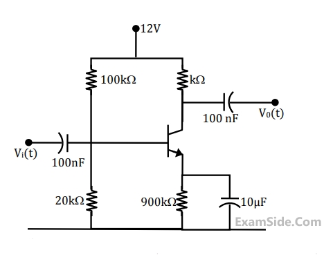
A small signal source, $V_i(t)=A \cos \left(10^5 t\right)+B \sin \left(10^7 t\right)$ is applied to a BJT circuit as shown in the Figure.
Assume zero source resistance, $V_{B E}=0.7 \mathrm{~V}, \beta_{\mathrm{dc}}=99$, Early voltage $=100 \mathrm{~V}$ and Thermal voltage $=25 \mathrm{mV}$. Effect of internal parasitic capacitances of the BJT may be neglected. Which expression is the best approximation of the output voltage $V_o(t)$ ?


Which of the following statements is/are true for a BJT with respect to its DC current gain $\beta$?
The base of an $n p n$ BJT $T 1$ has a linear doping profile $N_B(x)$ as shown below. The base of another $n p n$ BJT $T 2$ has a uniform doping $N_B$ of $10^{17} \mathrm{~cm}^{-3}$. All other parameters are identical for both the devices. Assuming that the hole density profile is the same as that of doping, the common - emitter current gain of $T 2$ is

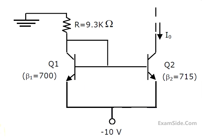
In the voltage regulator shown below, $V_I$ is the unregulated input at 15 V . Assume $V_{B E}=0.7 \mathrm{~V}$ and the base current is negligible for both the BJTs. If the regulated output $V_0$ is 9 V , the value of $R_2$ is $\_\_\_\_$ $\Omega$.

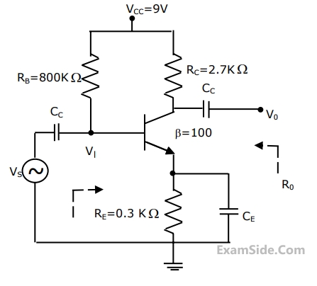
For the BJT in the amplifier shown below, $V_{B E}=0.7 \mathrm{~V}, \frac{k T}{q}=26 \mathrm{mV}$. Assume that the BJT output resistance ( $r_0$ ) is very high and the base current is negligible. The capacitors are also assumed to be short circuited at signal frequencies. The input $V_i$ is direct coupled. The low frequency voltage gain $\frac{V_0}{V_i}$ of the amplifier is


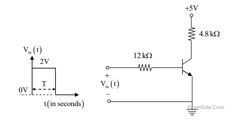
For the input vin(t)as shown in the figure, the transistor switches between the cut-off and saturation regions of operation, when T is large. Assume collector-to-emitter voltage saturation VCE(sat) = 0.2V and base-to-emitter voltage VBE = 0.7V. The minimum value of the common-base current gain$$\left( \alpha \right)$$ of the transistor for the switching should be _________.


The Value of DC current IE is
The mid-band voltage gain of the amplifier is approximately


If $${\beta _{DC}}$$ is increased by 10%, the collector-to emitter voltage drop
Under the DC conditions, the collector-to emitter voltage drop is
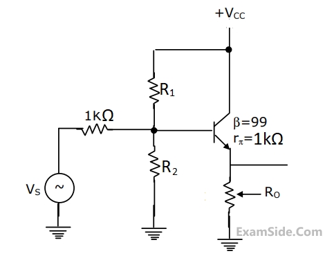
The small-signal gain of the amplifier $${{{V_c}} \over {{V_s}}}$$ is


Group - I
(a)Cascode amplifier(b)Differential Amplifier
(c)Darlington pair common-collector Amplifier
Group - II
(1)does not provide current gain(2)is a wide band Amplifier
(3)has very low input impedance Emitter Amplifier and very high current gain
(4)has very high input impedance and very high current gain
(5)Provides high common mode voltage Rejection
$$g\matrix{ c \cr m \cr } \left[ { \buildrel \Delta \over = {{{i_c}^c} \over {{v_{be}}^c}}} \right]$$ is given by


The output impedance is


Marks 5

(a)Draw the small signal equivalent circuit of the amplifier.
(b)Obtain an expression for zi.
(c)Obtain an expression for z0.
$${I_C}\, = \,1.3\,mA,\,{R_C}\, = \,2\,k\Omega ,\,{R_E}\, = \,500\,\Omega ,$$
$${V_T}\, = \,26\,mV,\,\beta \, = \,100,\,{V_{CC}}\, = \,15V,$$
$${V_s}\, = \,0.01\,\sin \left( {\omega t} \right)\,V\,and\,{C_b}\, = \,{C_C}\, = \,10\,\mu F.$$
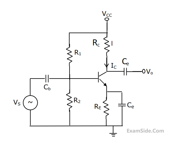
(a)What is the small-signal voltage gain, $${A_V} = {V_0}/{V_s}?$$
(b)What is the approximate $${A_{v,}}\,\,if\,\,{C_e}\,\,$$ is removed?
(c)What will $${V_0}\,be\,if\,{C_b}$$ is short circuited?
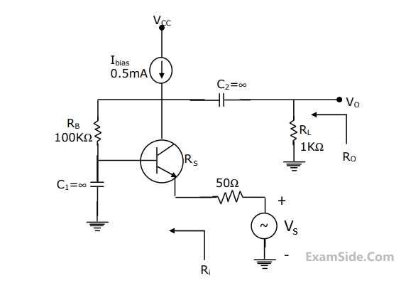
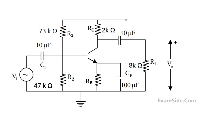
Determine the ac small-signal mid-band and voltage gain $$\left( {{V_o}/{V_s}} \right),$$ input resistance (R1, and output resistance (R0) of the circuit. Assume $${V_{T\,\,}} = \,\,26\,mV.$$

The N/W components have following values, RC = 2$$k\Omega $$,
RS = $$1.4k\Omega $$,
RE = $$100\Omega $$.
The transistor has specifications, $$\beta \,\, = \,\,100$$
and base spreading resistance $${r_{bb\,}}^1\, = \,100\Omega $$
Evaluate input resistance Ri for two cases. At a frequency of 10 kHz
(a)CE, the bypass capacitor across RE is 25 $$\mu F$$
(b)The bypass capacitor CE is removed leaving RE unbypassed.