1
GATE ECE 2016 Set 3
Numerical
+2
-0
Figures $${\rm I}$$ and $${\rm I}{\rm I}$$ show two MOS capacitor of unit area. The capacitor in Figure I has insulator materials X (of thickness t1 = 1 nm and dielectric constant $${\varepsilon _1}$$ = 4) and Y (of thickness t2 =3 nm and dielectric constant $${\varepsilon _2}$$ = 200). The capacitor in Figure $${\rm I}{\rm I}$$ has only insulator material X of thickness teq. If the capacitors are of equal capacitance, then the value of teq (in nm) is ______


Your input ____
2
GATE ECE 2016 Set 3
MCQ (Single Correct Answer)
+2
-0.6
In the circuit shown in the figure, the channel length modulation of all transistors is non-zero $$\left( {\lambda \ne 0} \right)$$. Also all transistors operate in saturation and have negligible body effect. The ac small
signal voltage gain $$\left( {{V_0}/{V_{in}}} \right)$$ of the circuit is


3
GATE ECE 2016 Set 3
Numerical
+2
-0
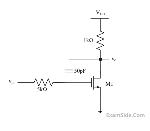
In the circuit shown in the figure, transistor M1 is in saturation and has transconductance
gm = 0.01 siemens. Ignoring internal parasitic capacitances and assuming the channel length
modulation $$\lambda $$ to be zero, the small signal input pole frequency (in kHz) is _____


Your input ____
4
GATE ECE 2016 Set 2
Numerical
+2
-0
Consider a long-channel NMOS transistor with source and body connected together. Assume that
the electron mobility is independent of VGS and VDS. Given,
gm = 0.5$$\mu {\rm A}/V$$ for VDS = 50 m V and VGS = 2V,
gd = $$8\mu {\rm A}/V$$ for VGS = 2 V and VDS = 0 V,
Where gm =$${{\partial {{\rm I}_D}} \over {\partial {V_{GS}}}}\,\,and\,\,{g_d}\,\, = \,{{\partial {{\rm I}_D}} \over {\partial {V_{DS}}}}$$
gm = 0.5$$\mu {\rm A}/V$$ for VDS = 50 m V and VGS = 2V,
gd = $$8\mu {\rm A}/V$$ for VGS = 2 V and VDS = 0 V,
Where gm =$${{\partial {{\rm I}_D}} \over {\partial {V_{GS}}}}\,\,and\,\,{g_d}\,\, = \,{{\partial {{\rm I}_D}} \over {\partial {V_{DS}}}}$$
The threshold voltage (in volts) of the transistor is
Your input ____
Questions Asked from IC Basics and MOSFET (Marks 2)
Number in Brackets after Paper Indicates No. of Questions
GATE ECE 2024 (1)
GATE ECE 2023 (1)
GATE ECE 2017 Set 2 (3)
GATE ECE 2017 Set 1 (1)
GATE ECE 2016 Set 3 (3)
GATE ECE 2016 Set 2 (2)
GATE ECE 2016 Set 1 (1)
GATE ECE 2015 Set 2 (1)
GATE ECE 2015 Set 3 (2)
GATE ECE 2015 Set 1 (2)
GATE ECE 2014 Set 1 (1)
GATE ECE 2014 Set 3 (3)
GATE ECE 2014 Set 2 (2)
GATE ECE 2013 (1)
GATE ECE 2012 (4)
GATE ECE 2009 (2)
GATE ECE 2008 (3)
GATE ECE 2007 (1)
GATE ECE 2006 (1)
GATE ECE 2004 (1)
GATE ECE 2003 (3)
GATE ECE Subjects
Signals and Systems
Representation of Continuous Time Signal Fourier Series Fourier Transform Continuous Time Signal Laplace Transform Discrete Time Signal Fourier Series Fourier Transform Discrete Fourier Transform and Fast Fourier Transform Discrete Time Signal Z Transform Continuous Time Linear Invariant System Discrete Time Linear Time Invariant Systems Transmission of Signal Through Continuous Time LTI Systems Sampling Transmission of Signal Through Discrete Time Lti Systems Miscellaneous
Network Theory
Control Systems
Digital Circuits
General Aptitude
Electronic Devices and VLSI
Analog Circuits
Engineering Mathematics
Microprocessors
Communications
Electromagnetics