1
GATE ECE 2017 Set 2
Numerical
+2
-0
A MOS capacitor is fabricated on p-type Si (silicon) where the metal work function is 4.1 eV
and electron affinity of Si is 4.0 eV, Ec - EF = 0.9 eV; where Ec and EF are conduction band minimum and the Fermi energy levels of Si, respectively. Oxide$${\varepsilon _r} = \,\,3.9,\,\,\,{\varepsilon _{0\,\,}}=\,8.85 \times {10^{ - 14}}$$ F/cm, oxide thickness $${t_{ox}} = 0.1\,\mu m$$
and electronic charge q = $$1.6 \times {10^{ - 19}}$$ C. If the measured flat band
voltage of the capacitor is –1V, then the magnitude of the fixed charge at the oxide semiconductor
interface, in nC/cm2, is __________.
Your input ____
2
GATE ECE 2017 Set 2
MCQ (Single Correct Answer)
+2
-0.6
Assuming that transistor M1 and M2 are identical and have a threshold voltage of 1V, the state of transistors M1 and M2 are respectively

3
GATE ECE 2017 Set 1
Numerical
+2
-0
For the circuit shown, assume that the NMOS transistor is in saturation. Its threshold voltage
Vtn = 1 V and its trans-conductance parameter $${\mu _n}{C_{ox}}\left( {{W \over L}} \right) = 1m{\rm A}/{V^2}.$$ Neglect channel length modulation and body bias effects. Under these conditions the drain current ID in mA is______.
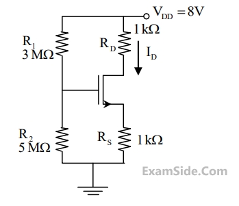
Your input ____
4
GATE ECE 2016 Set 2
Numerical
+2
-0
Consider a long-channel NMOS transistor with source and body connected together. Assume that
the electron mobility is independent of VGS and VDS. Given,
gm = 0.5$$\mu {\rm A}/V$$ for VDS = 50 m V and VGS = 2V,
gd = $$8\mu {\rm A}/V$$ for VGS = 2 V and VDS = 0 V,
Where gm =$${{\partial {{\rm I}_D}} \over {\partial {V_{GS}}}}\,\,and\,\,{g_d}\,\, = \,{{\partial {{\rm I}_D}} \over {\partial {V_{DS}}}}$$
gm = 0.5$$\mu {\rm A}/V$$ for VDS = 50 m V and VGS = 2V,
gd = $$8\mu {\rm A}/V$$ for VGS = 2 V and VDS = 0 V,
Where gm =$${{\partial {{\rm I}_D}} \over {\partial {V_{GS}}}}\,\,and\,\,{g_d}\,\, = \,{{\partial {{\rm I}_D}} \over {\partial {V_{DS}}}}$$
The threshold voltage (in volts) of the transistor is
Your input ____
GATE ECE Subjects
Browse all chapters by subject
Network Theory
Control Systems
Electronic Devices and VLSI
Analog Circuits
Digital Circuits
Microprocessors
Signals and Systems
Discrete Fourier Transform and Fast Fourier Transform Discrete Time Signal Fourier Series Fourier Transform Continuous Time Signal Laplace Transform Fourier Transform Representation of Continuous Time Signal Fourier Series Transmission of Signal Through Continuous Time LTI Systems Miscellaneous Sampling Continuous Time Linear Invariant System Discrete Time Linear Time Invariant Systems Discrete Time Signal Z Transform Transmission of Signal Through Discrete Time Lti Systems
Communications
Electromagnetics
General Aptitude