1
GATE ECE 1998
MCQ (Single Correct Answer)
+1
-0.3
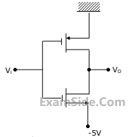
The threshold voltage for each transistor in Fig.2.5, is 2V. For this circuit to work as an inverter, Vi must take the values
2
GATE ECE 1997
MCQ (Single Correct Answer)
+1
-0.3
For the NMOS logic gate shown in figure, the logic function implemented is

3
GATE ECE 1997
MCQ (Single Correct Answer)
+1
-0.3
The gate delay of an NMOS inverter is dominated by charge time rather than discharge time because
4
GATE ECE 1997
MCQ (Single Correct Answer)
+1
-0.3
The inverter 74AL SO4 has the following specifications:
$${I_{OH}}{\,_{\max \,}} = \, - $$ 0.4mA, $${I_{OL}}$$ max = 8mA, $${I_{IH}}$$ max = $$\mu $$A , $${I_{IL\,}}_{\max \,}$$=0.1mA. The fan out based on the above will be
$${I_{OH}}{\,_{\max \,}} = \, - $$ 0.4mA, $${I_{OL}}$$ max = 8mA, $${I_{IH}}$$ max = $$\mu $$A , $${I_{IL\,}}_{\max \,}$$=0.1mA. The fan out based on the above will be
Questions Asked from Logic Families (Marks 1)
Number in Brackets after Paper Indicates No. of Questions
GATE ECE Subjects
Network Theory
Control Systems
Electronic Devices and VLSI
Analog Circuits
Digital Circuits
Microprocessors
Signals and Systems
Representation of Continuous Time Signal Fourier Series Discrete Time Signal Fourier Series Fourier Transform Discrete Time Signal Z Transform Continuous Time Linear Invariant System Transmission of Signal Through Continuous Time LTI Systems Discrete Time Linear Time Invariant Systems Sampling Continuous Time Signal Laplace Transform Discrete Fourier Transform and Fast Fourier Transform Transmission of Signal Through Discrete Time Lti Systems Miscellaneous Fourier Transform
Communications
Electromagnetics
General Aptitude