1
GATE ECE 2022
MCQ (More than One Correct Answer)
+1
-0
Select the correct statement(s) regarding CMOS implementation of NOT gates.
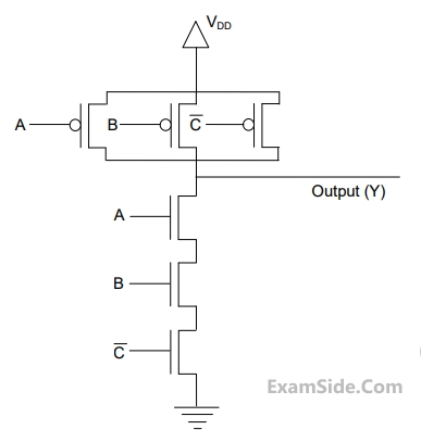
2
GATE ECE 2014 Set 4
MCQ (Single Correct Answer)
+1
-0.3
The output (Y) of the circuit shown in the figure is
3
GATE ECE 2009
MCQ (Single Correct Answer)
+1
-0.3
The full forms of the abbreviations TTL and COMS in reference to logic families are
4
GATE ECE 2005
MCQ (Single Correct Answer)
+1
-0.3
The transistors used in a portion of the TTL gate shown in figure have β=100. the base-emitter voltage of is 0.7V for a transistor in active region and 0.75V for a transistor in saturation . If the sink current I=1mA and the output is at logic 0,
then the current $${I_R}$$ I will be equal to

GATE ECE Subjects
Browse all chapters by subject
Control Systems
Engineering Mathematics
Analog Circuits
Network Theory
Electromagnetics
Electronic Devices and VLSI
Digital Circuits
Microprocessors
Signals and Systems
Discrete Fourier Transform and Fast Fourier Transform Discrete Time Signal Fourier Series Fourier Transform Continuous Time Signal Laplace Transform Fourier Transform Representation of Continuous Time Signal Fourier Series Transmission of Signal Through Continuous Time LTI Systems Miscellaneous Sampling Continuous Time Linear Invariant System Discrete Time Linear Time Invariant Systems Discrete Time Signal Z Transform Transmission of Signal Through Discrete Time Lti Systems
Communications
General Aptitude