1
GATE ECE 2009
MCQ (Single Correct Answer)
+2
-0.6
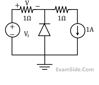
In the circuit below, the diode is ideal. The voltage V is given by
2
GATE ECE 2007
MCQ (Single Correct Answer)
+2
-0.6
A P+-N junction has a built-in potential of 0.8 V. The depletion layer width at a
reverse bias of 1.2V is 2 µm. For a reverse bias of 7.2 V, the depletion layer
width will be:
3
GATE ECE 2005
MCQ (Single Correct Answer)
+2
-0.6
The Zener diode in the regulator circuit shown in figure has a Zener voltage of
5.8 Volts and a Zener knee current of 0.5 mA. The maximum load current drawn
from this circuit ensuring proper functioning over the input voltage range
between 20 and 30 Volts, is

4
GATE ECE 2005
MCQ (Single Correct Answer)
+2
-0.6
A Silicon PN junction diode under reverse bias has depletion region of width 10
µm. The relative permittivity of Silicon, ɛr = 11.7 and the permittivity of free space ɛ0 = 8.854 × 10⁻¹² F/m.The depletion capacitance of the diode per square meter is
GATE ECE Subjects
Browse all chapters by subject
Control Systems
Engineering Mathematics
Analog Circuits
Network Theory
Electromagnetics
Electronic Devices and VLSI
Digital Circuits
Microprocessors
Signals and Systems
Discrete Fourier Transform and Fast Fourier Transform Discrete Time Signal Fourier Series Fourier Transform Continuous Time Signal Laplace Transform Fourier Transform Representation of Continuous Time Signal Fourier Series Transmission of Signal Through Continuous Time LTI Systems Miscellaneous Sampling Continuous Time Linear Invariant System Discrete Time Linear Time Invariant Systems Discrete Time Signal Z Transform Transmission of Signal Through Discrete Time Lti Systems
Communications
General Aptitude