1
GATE ECE 2025
MCQ (Single Correct Answer)
+2
-0.67
In the circuit shown, the identical transistors Q1 and Q2 are biased in the active region with $\beta=120$. The Zener diode is in the breakdown region with $V_Z=5 \mathrm{~V}$ and $I_Z=25 \mathrm{~mA}$. If $I_L=12 \mathrm{~mA}$ and $V_{E B 1}=V_{E B 2}=0.7 \mathrm{~V}$, then the values of $R_1$ and $R_2$ (in $\mathrm{k} \Omega$, rounded off to one decimal place) are ___________ , respectively.


2
GATE ECE 2024
MCQ (More than One Correct Answer)
+2
-0
Which of the following statements is/are true for a BJT with respect to its DC current gain $\beta$?
3
GATE ECE 2017 Set 1
Numerical
+2
-0
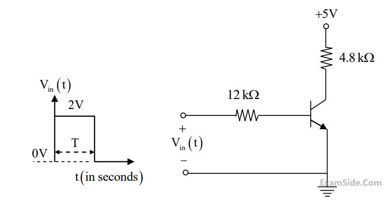
In the figure shown, the npn transistor acts as a switch.


For the input vin(t)as shown in the figure, the transistor switches between the cut-off and saturation regions of operation, when T is large. Assume collector-to-emitter voltage saturation VCE(sat) = 0.2V and base-to-emitter voltage VBE = 0.7V. The minimum value of the common-base current gain$$\left( \alpha \right)$$ of the transistor for the switching should be _________.
Your input ____
4
GATE ECE 2017 Set 1
Numerical
+2
-0
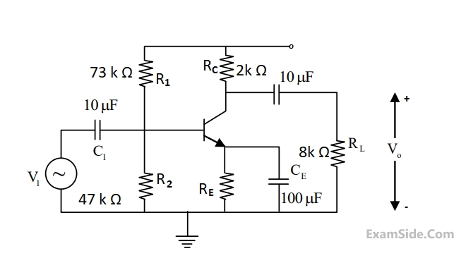
For the DC analysis of the Common-Emitter amplifier shown, neglect the base current and
assume that the emitter and collector current are equal. Given that VT = 25mV, VBE = 0.7V, and the BJT output r0 is practically infinite. Under these conditions the midband
voltage gain magnitude, av = $$\left| {{v_0}/{v_i}} \right|\,\,\,V/V,$$ is _____


Your input ____
Questions Asked from Bipolar Junction Transistor (Marks 2)
Number in Brackets after Paper Indicates No. of Questions
GATE ECE 2025 (1)
GATE ECE 2024 (1)
GATE ECE 2017 Set 1 (2)
GATE ECE 2017 Set 2 (1)
GATE ECE 2015 Set 2 (1)
GATE ECE 2015 Set 1 (1)
GATE ECE 2014 Set 4 (3)
GATE ECE 2014 Set 3 (1)
GATE ECE 2014 Set 1 (2)
GATE ECE 2013 (1)
GATE ECE 2012 (1)
GATE ECE 2011 (2)
GATE ECE 2009 (1)
GATE ECE 2008 (2)
GATE ECE 2007 (2)
GATE ECE 2006 (3)
GATE ECE 2005 (2)
GATE ECE 2004 (1)
GATE ECE 2003 (2)
GATE ECE 2000 (1)
GATE ECE 1996 (2)
GATE ECE 1992 (1)
GATE ECE 1991 (1)
GATE ECE 1990 (2)
GATE ECE 1989 (1)
GATE ECE 1988 (4)
GATE ECE Subjects
Network Theory
Control Systems
Electronic Devices and VLSI
Analog Circuits
Digital Circuits
Microprocessors
Signals and Systems
Representation of Continuous Time Signal Fourier Series Fourier Transform Continuous Time Signal Laplace Transform Discrete Time Signal Fourier Series Fourier Transform Discrete Fourier Transform and Fast Fourier Transform Discrete Time Signal Z Transform Continuous Time Linear Invariant System Discrete Time Linear Time Invariant Systems Transmission of Signal Through Continuous Time LTI Systems Sampling Transmission of Signal Through Discrete Time Lti Systems Miscellaneous
Communications
Electromagnetics
General Aptitude