4
Two n-channel MOSFETs, T1 and T2, are identical in all respects except that the width of T2 is double of T1. Both the transistor are biased in the saturation region of operation, but the gate overdrive voltage (VGS - VTH) of T2 is double that of T1, where VGS and VTH are the gate-to-source voltage and threshold voltage of the transistors, respectively. If the drain current and transconductance of T1 are ID1 and gm1 respectively ; the corresponding values of these two parameters for T2 are
5
A MOS capacitor is fabricated on p-type Si (silicon) where the metal work function is 4.1 eV
and electron affinity of Si is 4.0 eV, Ec - EF = 0.9 eV; where Ec and EF are conduction band minimum and the Fermi energy levels of Si, respectively. Oxide$${\varepsilon _r} = \,\,3.9,\,\,\,{\varepsilon _{0\,\,}}=\,8.85 \times {10^{ - 14}}$$ F/cm, oxide thickness $${t_{ox}} = 0.1\,\mu m$$
and electronic charge q = $$1.6 \times {10^{ - 19}}$$ C. If the measured flat band
voltage of the capacitor is –1V, then the magnitude of the fixed charge at the oxide semiconductor
interface, in nC/cm2, is __________.
10
A voltage VG is applied across a MOS capacitor with metal gate and p-type silicon substrate at
T=300 K. The inversion carrier density (in number of carriers per unit area) for VG = 0.8 V is $$2\,\, \times \,\,{10^{11}}\,\,\,\,\,\,c{m^{ - 2}}$$ . For $${V_G}\,\, = \,\,1.3\,\,V,$$ the inversion carrier density is $$4\,\,\, \times \,\,\,{10^{11}}\,\,\,\,c{m^{ - 2}}.$$ What is the value of the inversion carrier density for VG = 1.8 V?
12
Consider an n-channel metal oxide semiconductor field effect transistor (MOSFET) with a gate-to-source
voltage of 1.8 V. Assume that $${W \over L} = 4,{\mu _{\rm N}}{C_{ox}} = 70 \times {10^{ - 6}}{\rm A}{V^{ - 2}}$$ , the threshold voltage is 0.3V, and the channel length modulation parameter is 0.09 V-1, In the saturation region, the drain conductance (in micro siemens) is__________.
13
In a MOS capacitor with an oxide layer thickness of 10 nm, the maximum depletion layer thickness is 100 nm. The permittivities of the semiconductor and the oxide layer are $${\varepsilon _s}$$ and $${\varepsilon _{os}}$$ respectively. Asuuming $${\varepsilon _s}/{\varepsilon _{ox}} = 3$$ , the ratio of the maximum capacitance to the minimum capacitance of this MOS capacitor is________
15
The current in an enhancement mode NMOS transistor biased in saturation mode was measured to be 1 mA at a drain-source voltage of 5 V. When the drain-source voltage was increased to 6 V while keeping gate-source voltage same, the drain current increased to 1.02 mA. Assume that drain to source saturation voltage is much smaller than the applied drain-source voltage. The channel length modulation p[arameter $$\lambda $$ (in V-1) is _______
16
A MOSFET in saturation has a drain current of 1 mA for VDS =0.5V. If the channel length modulation coefficient is 0.05 V-1, the output resistance (in k$$\Omega $$) of the MOSFET is______
18
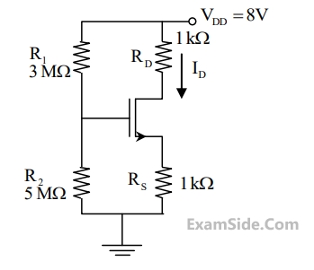
A depletion type N -channel MOSFET is biased in its linear region for use as a voltage controlled resistor. Assume threshold voltage VTH = -0.5 V, VGS = 2.0 V, VDS = 5 V, W/L=100, COX=10-8 F/cm2 and $${\mu _n}$$ = 800 cm2/V-s. The value of the resistance of the voltage controlled resistor (in $$\Omega $$ ) is _____.
19
An ideal MOS capacitor has boron doping concentration of 1015 cm-3 in the substrate. When a gate voltage is applied, a depletion region of width 0.5 $$\mu m$$ is formed with a surface (channel) potential of 0.2V. Given that $${\varepsilon _0} = 80854 \times {10^{ - 14}}F/cm$$ and the relative permittivities of silicon and silicon dioxide are 12 and 4, respectively, the peak electric field (in V/ $$\mu m$$ ) in the oxide region is ______
20
The slope of the ID vs. VGS curve of an n-channel MOSFET in linear region is 10-3$${\Omega ^{ - 1}}$$ at VDS = 0.1V. For the same device, neglecting channel length modulation, the slope of the $$\sqrt {{{\rm I}_D}} $$ vs. V GS curve (in $$\sqrt A /V$$ ) under saturation region is approximately ______.
27
The source of a silicon (ni = 1010 per cm3) n - channel MOS transistor has an aewa of 1 sq $$\mu m$$ and a depth of 1 $$\mu m$$ . If the dopant density in the source is 1019/cm3, the number of holes in the source region with the above volume is approximately
31
The measured transconductance gm of an NMOS transistor operating in the linear
region is plotted against the gate voltage VG at constant drain voltage VD. Which
of the following figures represents the expected dependence of gm on VG?
35
An n-channel depletion MOSFET has following two points on its ID − VGS curve:
(i) VGS = 0 at ID = 12 mA and
(ii) VGS = - 6 Volts at ID = 0
Which of the following Q-points will give the highest trans-conductance gain for
small signals?
36
The drain of an n-channel MOSFET is shorted to the gate so that VGS = VDS. The
threshold voltage (VT) of MOSFET is 1 V. If the drain current (ID) is 1 mA for VGS =
2 V, then for VGS = 3 V, ID is
37
If P is Passivation, Q is n-well implant, R is metallization and S is source/drain
diffusion, then the order in which they are carried out in a standard n-well CMOS
fabrication process, is
38
For an n-channel enhancement type MOSFET, if the source is connected at a
higher potential than that of the bulk (i.e. VSB > 0), the threshold voltage VT of
the MOSFET will
39
When the gate-to-source voltage (VGS) of a MOSFET with threshold voltage of
400 mV, working in saturation is 900 mV, the drain current is observed to be 1
mA. Neglecting the channel width modulation effect and assuming that the
MOSFET is operating at saturation, the drain current for an applied VGS of 1400
mV is
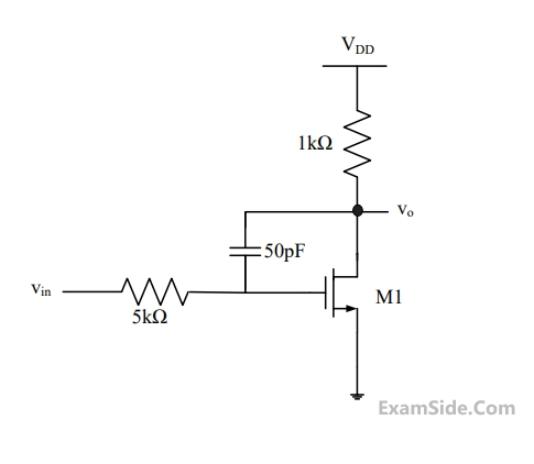
 The logic implemented by the circuit is


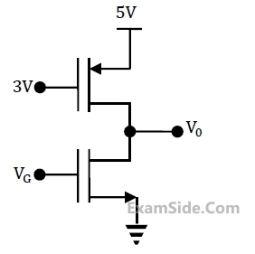
 The current Ix is related to Ibias as
