1
GATE ECE 2007
MCQ (Single Correct Answer)
+1
-0.3
In a p+n junction diode under reverse bias, the magnitude of electric field is
maximum at
2
GATE ECE 2002
MCQ (Single Correct Answer)
+1
-0.3
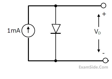
In the figure, a silicon diode is carrying a constant current of 1 mA. When the
temperature of the diode is 20°C, VD is found to be 700 mV. If the temperature
rises to 40°C, VD becomes approximately equal to
3
GATE ECE 1998
MCQ (Single Correct Answer)
+1
-0.3
The static characteristic of an adequately forward biased p-n junction is a straight
line, if the plot is of
4
GATE ECE 1998
MCQ (Single Correct Answer)
+1
-0.3
For small signal a.c. operation, a practical forward biased diode can be modeled
as
GATE ECE Subjects
Browse all chapters by subject
General Aptitude
Network Theory
Microprocessors
Signals and Systems
Discrete Time Signal Fourier Series Fourier Transform Continuous Time Signal Laplace Transform Fourier Transform Discrete Fourier Transform and Fast Fourier Transform Representation of Continuous Time Signal Fourier Series Discrete Time Linear Time Invariant Systems Transmission of Signal Through Continuous Time LTI Systems Transmission of Signal Through Discrete Time Lti Systems Miscellaneous Continuous Time Linear Invariant System Discrete Time Signal Z Transform Sampling
Electromagnetics
Digital Circuits
Electronic Devices and VLSI
Control Systems
Communications
Engineering Mathematics