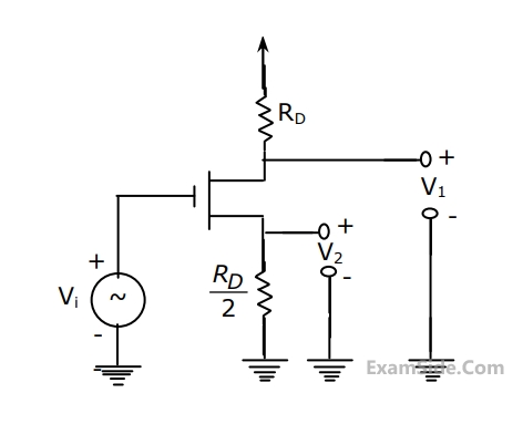
For the transistor $M_1$ in the circuit shown in the figure, $\mu_n C_{o x}=100 \mu \mathrm{~A} / V^2$ and $\frac{W}{L}=10$, where $\mu_n$ is the mobility of electron, $C_{o x}$ is the oxide capacitance per unit area. $W$ is the width and $L$ is the length.
 The channel length modulation coefficient is ignored. If the gate-to-source voltage $V_{G S}$ is 1 V to keep the transistor at the edge of saturation. Then the threshold voltage of the transistor (rounded off to one decimal place) is $\_\_\_\_$ V.
In the circuit shown in the figure, the transistors $M_1$ and $M_2$ are operating in saturation. The channel length
modulation coefficients of both the transistors are non-zero. The transconductance of the MOSFETs $M_1$ and $M_2$ are $g_{m 1}$ and $g_{m 2}$, respectively, and the internal resistance of the MOSFETs $M_1$ and $M_2$ are $r_{01}$ and $r_{02}$ respectively.
 Ignoring the body effect, the ac small signal voltage gain ( $d V_{\text {out }} / d V_{\text {in }}$ ) of the circuit is
GATE ECE Subjects
Browse all chapters by subject