1
GATE ECE 2014 Set 3
Numerical
+1
-0
In the circuit shown, the PNP transistor has $$\left|{\mathrm V}_\mathrm{BE}\right|=0.7\;\mathrm V$$ and β = 50. Assume that RB = 100 kΩ.
For V0 to be 5 V, the value of RC ( in kΩ) is _____________.
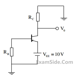
Your input ____
2
GATE ECE 2014 Set 4
MCQ (Single Correct Answer)
+1
-0.3
If the emitter resistance in a common-emitter voltage amplifier is not bypassed, it will
3
GATE ECE 2014 Set 2
Numerical
+1
-0
A cascade connection of two voltage amplifiers A1 and A2 is shown in the figure. The open-loop
gain Av0, input resistance Rin, and output resistance R0 for A1 and A2 are as follows:
A1: Av0 = 10,Rin = 10 kΩ ,R0 =1 kΩ
A2 : Av0 = 5,Rin = 5 kΩ , R0 = 200 Ω
The approximate overall voltage gain $$\frac{{\mathrm V}_\mathrm{out}}{{\mathrm V}_\mathrm{in}}$$ is ______.
A1: Av0 = 10,Rin = 10 kΩ ,R0 =1 kΩ
A2 : Av0 = 5,Rin = 5 kΩ , R0 = 200 Ω
The approximate overall voltage gain $$\frac{{\mathrm V}_\mathrm{out}}{{\mathrm V}_\mathrm{in}}$$ is ______.
Your input ____
4
GATE ECE 2012
MCQ (Single Correct Answer)
+1
-0.3
The current ib through the base of a silicon npn transistor is
$$1\;+\;0.1\;\cos\left(10000\;\mathrm\pi\;\mathrm t\right)$$ mA
. At 300 K,
the $$r_\mathrm\pi$$ in the small signal model of the transistor is

GATE ECE Subjects
Browse all chapters by subject
Control Systems
Engineering Mathematics
Analog Circuits
Network Theory
Electromagnetics
Electronic Devices and VLSI
Digital Circuits
Microprocessors
Signals and Systems
Discrete Fourier Transform and Fast Fourier Transform Discrete Time Signal Fourier Series Fourier Transform Continuous Time Signal Laplace Transform Fourier Transform Representation of Continuous Time Signal Fourier Series Transmission of Signal Through Continuous Time LTI Systems Miscellaneous Sampling Continuous Time Linear Invariant System Discrete Time Linear Time Invariant Systems Discrete Time Signal Z Transform Transmission of Signal Through Discrete Time Lti Systems
Communications
General Aptitude