Semiconductor · Physics · JEE Main
MCQ (Single Correct Answer)
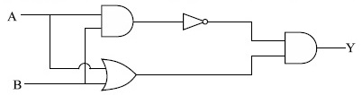
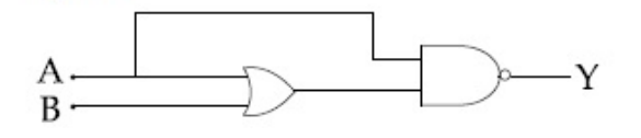
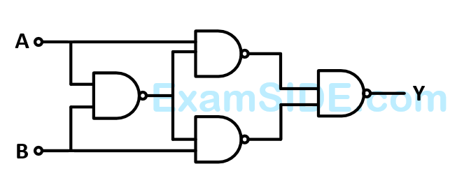
$$ \text { The output } Y \text { for the given inputs } A \text { and } B \text { to the circuit is : } $$

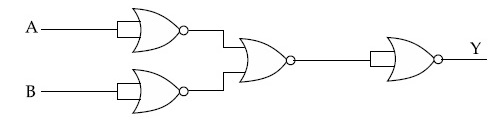
Refer to the logic circuit given below. For two inputs ( $A=1, B=1$ ) and ( $A=0, B=1$ ), output ( Y ) will be $\_\_\_\_$ .

The maximum rated power of the LED is 2 mW and it is used in the circuit with input voltage of 5 V as shown in the figure below. The current through resistance $R_S$ is 0.5 mA .
The minimum value of the resistance of $R_S$, to ensure that the LED is not damaged is $\_\_\_\_$ $\mathrm{k} \Omega$.

In a semiconductor $p$-n diode, the doping concentrations on $p$-side and $n$-side are $10^{15}$ atoms $/ \mathrm{cm}^3$ and $10^{18}$ atoms $/ \mathrm{cm}^3$, respectively. Which one of the following statements is true?
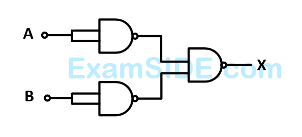
For the given logic circuit, which of the following inputs combination will make both LED-1 and LED-2 to glow?

Given below are two statements: one is labelled as Assertion A and the other is labelled as Reason $\mathbf{R}$
Assertion A : A diode under reverse-biased condition provides very small current which is nearly independent of voltage until a critical limit at which the current increases drastically.
Reason R : Below the critical voltage limit, only majority charge carriers flow which increases drastically above critical voltage.
choose the correct answer from the options given below
Two 4 bits binary numbers, $A=1101$ and $B=1010$ are given in the inputs of a logic circuit shown in figure below. The output $(Y)$ will be :

Consider a circuit consisting of a capacitor $(20 \mu \mathrm{~F})$, resistor $(100 \Omega)$ and two identical diodes as shown in figure. The resistance of diode under forward biasing condition is $10 \Omega$. The time constant of the circuit is $\alpha \times 10^{-3} \mathrm{~s}$. The value of $\alpha$ is $\_\_\_\_$

If X and Y are the inputs, the given circuit works as _________.

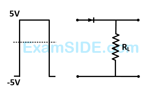
For the given circuit (shown in part (A)) the time dependent input voltage $v_{in}(t)$ and corresponding output $v_{o}(t)$ are shown in part (B) and part (C), respectively. Identify the components that are used in the circuit between points X and Y.


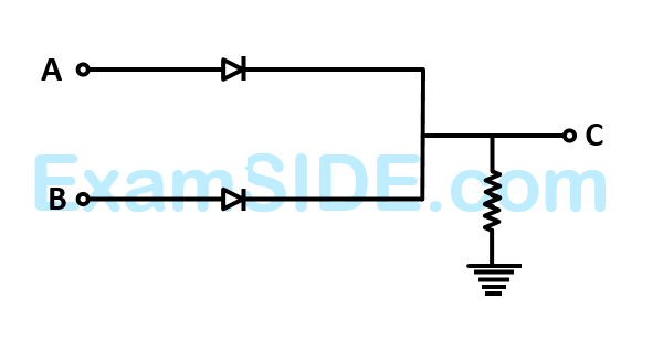
Two p-n junction diodes $D_1$ and $D_2$ are connected as shown in figure. $A$ and $B$ are input signals and $C$ is the output. The given circuit will function as a ________.

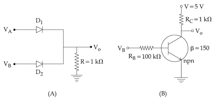
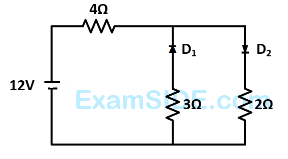
Assuming in forward bias condition there is a voltage drop of 0.7 V across a silicon diode, the current through diode $D_1$ in the circuit is $\_\_\_\_$ mA .
(Assume all diodes in the given circuit are identical)

$$ \text { Identify the correct truth table of the given logic circuit. } $$

$$ \text { For the given logic gate circuit, which of the following is the correct truth table? } $$

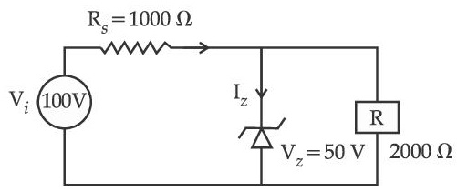
The following diagram shows a Zener diode as a voltage regulator. The Zener diode is rated at $V_z=5 \mathrm{~V}$ and the desired current in load is 5 mA . The unregulated voltage source can supply upto 25 V . Considering the Zener diode can withstand four times of the load current, the value of resistor $R_s$ (shown in circuit) should be $\_\_\_\_$ $\Omega$.

The correct truth table for the given input data of the following logic gate is :

Find the correct combination of $\mathrm{A}, \mathrm{B}, \mathrm{C}$ and D inputs which can cause the LED to glow.

The charge stored by the capacitor C in the given circuit in the steady state is __________ µC.

$$ \text { The given circuit works as : } $$

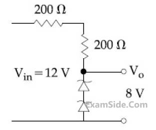
The output voltage in the following circuit is (Consider ideal diode case)

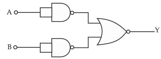
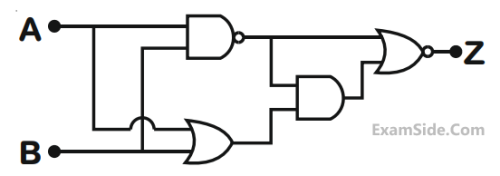
Consider the following logic circuit.

The output is Y = 0 when :
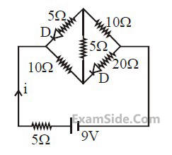
In the following circuit, the reading of the ammeter will be
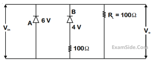
$($ Take Zener breakdown voltage $=4 \mathrm{~V})$

Consider a n-type semiconductor in which $\mathrm{n}_{\mathrm{e}}$ and $\mathrm{n}_{\mathrm{h}}$ are number of electrons and holes, respectively.
(A) Holes are minority carriers
(B) The dopant is a pentavalent atom
(C) $\mathrm{n}_{\mathrm{e}} \mathrm{n}_{\mathrm{h}} \neq \mathrm{n}_i^2$
(where $\mathrm{n}_i$ is number of electrons or holes in semiconductor when it is intrinsic form)
(D) $\mathrm{n}_{\mathrm{e}} \mathrm{n}_{\mathrm{h}} \geqslant \mathrm{n}_i^2$
(E) The holes are not generated due to the donors
Choose the correct answer from the options given below :
The Boolean expression $\mathrm{Y}=A \bar{B} C+\bar{A} \bar{C}$ can be realised with which of the following gate configurations.
A. One 3-input AND gate, 3 NOT gates and one 2-input OR gate, One 2-input AND gate,
B. One 3 -input AND gate, 1 NOT gate, One 2 -input NOR gate and one 2 -input OR gate
C. 3 -input OR gate, 3 NOT gates and one 2 -input AND gate
Choose the correct answer from the options given below:
$$ \text {The truth table corresponding to the circuit given below is: } $$

$$ \text { Choose the correct logic circuit for the given truth table having inputs } A \text { and } B \text {. } $$
| Inputs | Output | ||
|---|---|---|---|
| A | B | Y | |
| 0 | 0 | 0 | |
| 0 | 1 | 0 | |
| 1 | 0 | 1 | |
| 1 | 1 | 1 | |
$$ \text { In the digital circuit shown in the figure, for the given inputs the } P \text { and } Q \text { values are : } $$

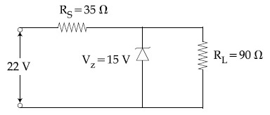
A zener diode with 5 V zener voltage is used to regulate an unregulated dc voltage input of 25 V . For a $400 \Omega$ resistor connected in series, the zener current is found to be 4 times load current. The load current $\left(I_L\right)$ and load resistance $\left(R_L\right)$ are :
The truth table for the circuit given below is:


For the circuit shown above, equivalent GATE is :
Which of the following circuits has the same output as that of the given circuit?

The output of the circuit is low (zero) for :

(A) $X=0, Y=0$
(B) $X=0, Y=1$
(C) $X=1, Y=0$
(D) $X=1, Y=1$
Choose the correct answer from the options given below :
Consider the following statements :
A. The junction area of solar cell is made very narrow compared to a photo diode.
B. Solar cells are not connected with any external bias.
C. LED is made of lightly doped p-n junction.
D. Increase of forward current results in continuous increase of LED light intensity.
E. LEDs have to be connected in forward bias for emission of light.
Choose the correct answer from the options given below :
What is the current through the battery in the circuit shown below?

Refer to the circuit diagram given in the figure. which of the following observations are correct?
A. Total resistance of circuit is $6 \Omega$
B. Current in Ammeter is 1 A
C. Potential across $A B$ is 4 Volts.
D. Potential across CD is 4 Volts
E. Total resistance of the circuit is $8 \Omega$.
Choose the correct answer from the options given below:


To obtain the given truth table, following logic gate should be placed at G :
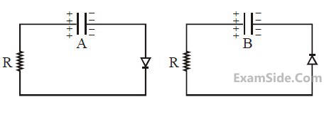
Which of the following circuits represents a forward biased diode?

Choose the correct answer from the options given below:

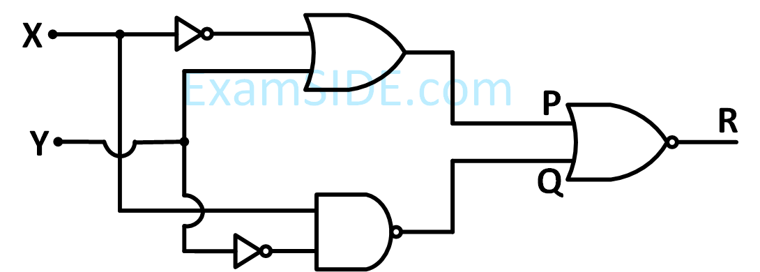
In the truth table of the above circuit the value of X and Y are :
The $$I$$-$$V$$ characteristics of an electronic device shown in the figure. The device is :

A light emitting diode (LED) is fabricated using GaAs semiconducting material whose band gap is $$1.42 \mathrm{~eV}$$. The wavelength of light emitted from the LED is :
The output $$\mathrm{Y}$$ of following circuit for given inputs is :

The acceptor level of a p-type semiconductor is $$6 \mathrm{~eV}$$. The maximum wavelength of light which can create a hole would be : Given $$\mathrm{hc}=1242 \mathrm{~eV} \mathrm{~nm}$$.
The correct truth table for the following logic circuit is :

The output (Y) of logic circuit given below is 0 only when :

Following gates section is connected in a complete suitable circuit.

For which of the following combination, bulb will glow (ON) :
Which of the diode circuit shows correct biasing used for the measurement of dynamic resistance of p-n junction diode :
Identify the logic gate given in the circuit :

The value of net resistance of the network as shown in the given figure is :


The output of the given circuit diagram is -
Identify the logic operation performed by the given circuit.


In the given circuit, the voltage across load resistance (R$$_L$$) is :
A Zener diode of breakdown voltage $$10 \mathrm{~V}$$ is used as a voltage regulator as shown in the figure. The current through the Zener diode is :

The truth table for this given circuit is :

In the given circuit, the breakdown voltage of the Zener diode is $$3.0 \mathrm{~V}$$. What is the value of $$\mathrm{I}_{\mathrm{z}}$$ ?

The truth table of the given circuit diagram is :

Which of the following circuits is reverse - biased?

The output from NAND gate having inputs A and B given below will be,

For the following circuit and given inputs A and B, choose the correct option for output '$$Y$$'

In an n-p-n common emitter (CE) transistor the collector current changes from 5 $$\mathrm{mA}$$ to $$16 \mathrm{~mA}$$ for the change in base current from $$100~ \mu \mathrm{A}$$ and $$200 ~\mu \mathrm{A}$$, respectively. The current gain of transistor is __________.
The logic operations performed by the given digital circuit is equivalent to:

The logic performed by the circuit shown in figure is equivalent to :

If each diode has a forward bias resistance of $$25 ~\Omega$$ in the below circuit,

Which of the following options is correct :
A zener diode of power rating 1.6 W is to be used as voltage regulator. If the zener diode has a breakdown of 8V and it has to regulate voltage fluctuating between 3 V and 10 V. The value of resistance Rs for safe operation of diode will be

For a given transistor amplifier circuit in $$\mathrm{CE}$$ configuration $$\mathrm{V}_{\mathrm{CC}}=1 \mathrm{~V}, \mathrm{R}_{\mathrm{C}}=1 ~\mathrm{k} \Omega, \mathrm{R}_{\mathrm{b}}=100 ~\mathrm{k} \Omega$$ and $$\beta=100$$. Value of base current $$\mathrm{I}_{\mathrm{b}}$$ is

For the logic circuit shown, the output waveform at $$\mathrm{Y}$$ is:

Given below are two statements: one is labelled as Assertion A and the other is labelled as Reason R
Assertion A: Diffusion current in a p-n junction is greater than the drift current in magnitude if the junction is forward biased.
Reason R: Diffusion current in a p-n junction is from the $$\mathrm{n}$$-side to the p-side if the junction is forward biased.
In the light of the above statements, choose the most appropriate answer from the options given below
Name the logic gate equivalent to the diagram attached

The resistivity $$(\rho)$$ of semiconductor varies with temperature. Which of the following curve represents the correct behaviour :
Choose the correct statement about Zener diode :
Match List I with List II:
| List I | List II | ||
|---|---|---|---|
| A. | Intrinsic semiconductor | I. | Fermi-level near the valence bond |
| B. | n-type semiconductor | II. | Fermi-level in the middle of valence and conduction band. |
| C. | p-type semiconductor | III. | Fermi-level near the conduction band |
| D. | Metals | IV. | Fermi-level inside the conduction band |
Choose the correct answer from the options given below :
Given below are two statements :
Statement I: In a typical transistor, all three regions emitter, base and collector have same doping level.
Statement II: In a transistor, collector is the thickest and base is the thinnest segment.
In the light of the above statements, choose the most appropriate answer from the options given below.
The effect of increase in temperature on the number of electrons in conduction band ($$\mathrm{n_e}$$) and resistance of a semiconductor will be as:
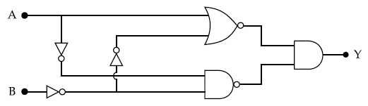
The output $Y$ for the inputs $A$ and $B$ of circuit is given by

Truth table of the shown circuit is:
The output waveform of the given logical circuit for the following inputs A and B as shown below, is :

For the given logic gates combination, the correct truth table will be

Which one of the following statement is not correct in the case of light emitting diodes?
A. It is a heavily doped p-n junction.
B. It emits light only when it is forward biased.
C. It emits light only when it is reverse biased.
D. The energy of the light emitted is equal to or slightly less than the energy gap of the semiconductor used.
Choose the correct answer from the options given below:
Statement I : When a Si sample is doped with Boron, it becomes P type and when doped by Arsenic it becomes N-type semi conductor such that P-type has excess holes and N-type has excess electrons.
Statement II : When such P-type and N-type semi-conductors, are fused to make a junction, a current will automatically flow which can be detected with an externally connected ameter.
In the light of above statements, choose the most appropriate answer from the options given below
Given below are two statements : one is labelled as Assertion A and the other is labelled as Reason R
Assertion A : Photodiodes are used in forward bias usually for measuring the light intensity.
Reason R : For a p-n junction diode, at applied voltage V the current in the forward bias is more than the current in the reverse bias for $$\mathrm{|{V_z}| > \pm v \ge |{v_0}|}$$ where $$\mathrm{v_0}$$ is the threshold voltage and $$\mathrm{V_z}$$ is the breakdown voltage.
In the light of the above statements, choose the correct answer from the options given below

The logic gate equivalent to the given circuit diagram is :
Given below are two statements : one is labelled as Assertion A and the other is labelled as Reason R
Assertion A : Photodiodes are preferably operated in reverse bias condition for light intensity measurement.
Reason R : The current in the forward bias is more than the current in the reverse bias for a $$p-n$$ junction diode.
In the light of the above statements, choose the correct answer from the options given below :
An n.p.n transistor with current gain $$\beta=100$$ in common emitter configuration is shown in figure. The output voltage of the amplifier will be

Identify the solar cell characteristics from the following options :
For a constant collector-emitter voltage of $$8 \mathrm{~V}$$, the collector current of a transistor reached to the value of $$6 \mathrm{~mA}$$ from $$4 \mathrm{~mA}$$, whereas base current changed from $$20 \,\mu \mathrm{A}$$ to $$25 \,\mu \mathrm{A}$$ value. If transistor is in active state, small signal current gain (current amplification factor) will be :
A logic gate circuit has two inputs A and B and output Y. The voltage waveforms of A, B and Y are shown below.

The logic gate circuit is :
In the circuit, the logical value of $$A=1$$ or $$B=1$$ when potential at $$A$$ or $$B$$ is $$5 \mathrm{~V}$$ and the logical value of $$A=0$$ or $$B=0$$ when potential at $$A$$ or $$B$$ is $$0 \mathrm{~V}$$.

The truth table of the given circuit will be :
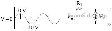
In the given circuit the input voltage Vin is shown in figure. The cut-in voltage of p-n junction diode (D1 or D2) is 0.6 V. Which of the following output voltage (V0) waveform across the diode is correct?

In the following circuit, the correct relation between output (Y) and inputs A and B will be :

For using a multimeter to identify diode from electrical components, choose the correct statement out of the following about the diode :
Given below are two statements : One is labelled as Assertion A and the other is labelled as Reason R.
Assertion A : n-p-n transistor permits more current than a p-n-p transistor.
Reason R : Electrons have greater mobility as a charge carrier.
Choose the correct answer from the options given below :
For a transistor to act as a switch, it must be operated in
Identify the correct Logic Gate for the following output (Y) of two inputs A and B.

The positive feedback is required by an amplifier to act an oscillator. The feedback here means :
The I-V characteristics of a p-n junction diode in forward bias is shown in the figure. The ratio of dynamic resistance, corresponding to forward bias voltage of 2 V and 4 V respectively, is :

Identify the logic operation performed by the given circuit:

The photodiode is used to detect the optical signals. These diodes are preferably operated in reverse biased mode because :

To get a steady dc output from the pulsating voltage received from a full wave rectifier we can connect a capacitor across the output parallel to the load RL.
Statement - II :
To get a steady dc output from the pulsating voltage received from a full wave rectifier we can connect an inductor in series with RL.
In the light of the above statements, choose the most appropriate answer from the options given below :


Statement II : The n-type semiconductor has net negative charge.
In the light of the above statements, choose the most appropriate answer from the options given below :


[h = 6.63 $$\times$$ 10$$-$$34 Js and c = 3 $$\times$$ 108 ms$$-$$1]


The logic circuit shown above is equivalent to :
Statement I : PN junction diodes can be used to function as transistor, simply by connecting two diodes, back to back, which acts as the base terminal.
Statement II : In the study of transistor, the amplification factor $$\beta$$ indicates ratio of the collector current to the base current.
In the light of the above statements, choose the correct answer from the options given below.

(Vinput = 0 V at t = 0)
(figures are qualitative)

zener diode used in the given circuit as 6V.
For the input voltage shown in figure below,
the time variation of the output voltage is:
(Graphs drawn are schematic and not to scale)
Planck’s constant h = 6.63 $$ \times $$ 10–34 J.s. Speed of light c = 3 $$ \times $$ 108 m/s
input (A, B) are (1, 0), (0, 0), (1, 1,), (0, 1)


The current IZ through the Zener is :


$$\beta $$ is curret gain, $${{\rm I}_B},{{\rm I}_C}$$ and $${{\rm I}_E}$$ are respectively base, collector and emitter currents.

(Take charge of electronas 1.6 $$ \times $$ 10 $$-$$19 c)

| A | B | Y |
|---|---|---|
| 0 | 0 | 0 |
| 0 | 1 | 1 |
| 1 | 0 | 1 |
| 1 | 1 | 1 |


Output is

The current $$(I)$$ in the resistor $$(R)$$ can be shown by :
The circuit represents
Then the output signal across $${R_L}$$ will be
Numerical
A diode has Zener voltage of 10 V and maximum power dissipation of 0.5 W , then the minimum resistance to be used in series with this diode for safety when it is connected to a 25 V power supply is $\_\_\_\_$ $\Omega$.
A voltage regulating circuit consisting of Zener diode, having break-down voltage of 10 V and maximum power dissipation of 0.4 W , is operated at 15 V . The approximate value of protective resistance in this circuit is $\_\_\_\_$ $\Omega$.
A potential divider circuit is connected with a dc source of $$20 \mathrm{~V}$$, a light emitting diode of glow in voltage $$1.8 \mathrm{~V}$$ and a zener diode of breakdown voltage of $$3.2 \mathrm{~V}$$. The length (PR) of the resistive wire is $$20 \mathrm{~cm}$$. The minimum length of PQ to just glow the LED is _________ $$\mathrm{cm}$$.

From the given transfer characteristic of a transistor in $$\mathrm{CE}$$ configuration, the value of power gain of this configuration is $$10^{x}$$, for $$\mathrm{R}_{\mathrm{B}}=10 ~\mathrm{k} \Omega$$, and $$\mathrm{R}_{\mathrm{C}}=1 ~\mathrm{k} \Omega$$. The value of $$x$$ is __________.

A $$8 \mathrm{~V}$$ Zener diode along with a series resistance $$\mathrm{R}$$ is connected across a $$20 \mathrm{~V}$$ supply (as shown in the figure). If the maximum Zener current is $$25 \mathrm{~mA}$$, then the minimum value of R will be _______ $$\Omega$$.

If the potential barrier across a p-n junction is $$0.6 \mathrm{~V}$$. Then the electric field intensity, in the depletion region having the width of $$6 \times 10^{-6} \mathrm{~m}$$, will be __________ $$\times 10^{5} \mathrm{~N} / \mathrm{C}$$.
The typical transfer characteristics of a transistor in CE configuration is shown in figure. A load resistor of $$2 \,k \Omega$$ is connected in the collector branch of the circuit used. The input resistance of the transistor is $$0.50 \,\mathrm{k} \Omega$$. The voltage gain of the transistor is ______________.

In the circuit shown below, maximum zener diode current will be _________ $$\mathrm{mA}$$.

Two ideal diodes are connected in the network as shown in figure. The equivalent resistance between A and B is __________ $$\Omega$$.

The energy band gap of semiconducting material to produce violet (wavelength = 4000$$\mathop A\limits^o $$ ) LED is ______________ $$\mathrm{eV}$$. (Round off to the nearest integer).
The circuit diagram used to study the characteristic curve of a zener diode is connected to variable power supply (0 $$-$$ 15 V) as shown in figure. A zener diode with maximum potential Vz = 10 V and maximum power dissipation of 0.4 W is connected across a potential divider arrangement. The value of resistance RP connected in series with the zener diode to protect it from the damage is ________________ $$\Omega$$.

A potential barrier of 0.4 V exists across a p-n junction. An electron enters the junction from the n-side with a speed of 6.0 $$\times$$ 105 ms$$-$$1. The speed with which electron enters the p side will be $${x \over 3} \times {10^5}$$ ms$$-$$1 the value of x is _____________.
(Given mass of electron = 9 $$\times$$ 10$$-$$31 kg, charge on electron = 1.6 $$\times$$ 10$$-$$19 C.)
A transistor is used in an amplifier circuit in common emitter mode. If the base current changes by 100 $$\mu$$A, it brings a change of 10 mA in collector current. If the load resistance is 2 k$$\Omega$$ and input resistance is 1 k$$\Omega$$, the value of power gain is x $$\times$$ 104. The value of x is _____________.
A zener of breakdown voltage Vz = 8 V and maximum zener current, IZM = 10 mA is subjectd to an input voltage Vi = 10 V with series resistance R = 100 $$\Omega$$. In the given circuit RL represents the variable load resistance. The ratio of maximum and minimum value of RL is _____________.

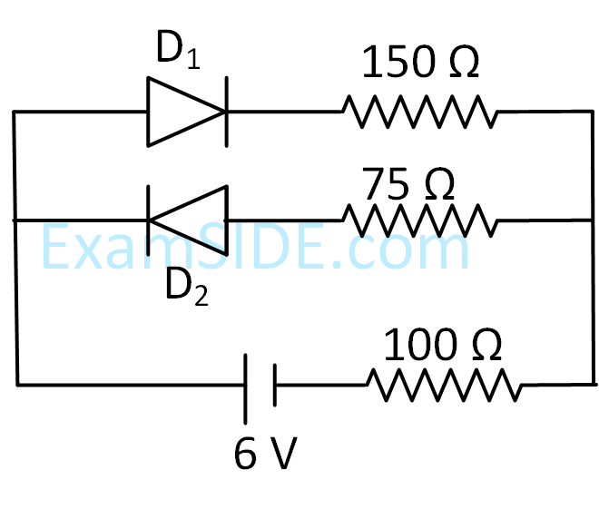
The cut-off voltage of the diodes (shown in figure) in forward bias is 0.6 V. The current through the resister of 40 $$\Omega$$ is __________ mA.

As per the given circuit, the value of current through the battery will be ____________ A.

In an experiment of CE configuration of n-p-n transistor, the transfer characteristics are observed as given in figure.

If the input resistance is 200 $$\Omega$$ and output resistance is 60 $$\Omega$$, the voltage gain in this experiment will be ____________.
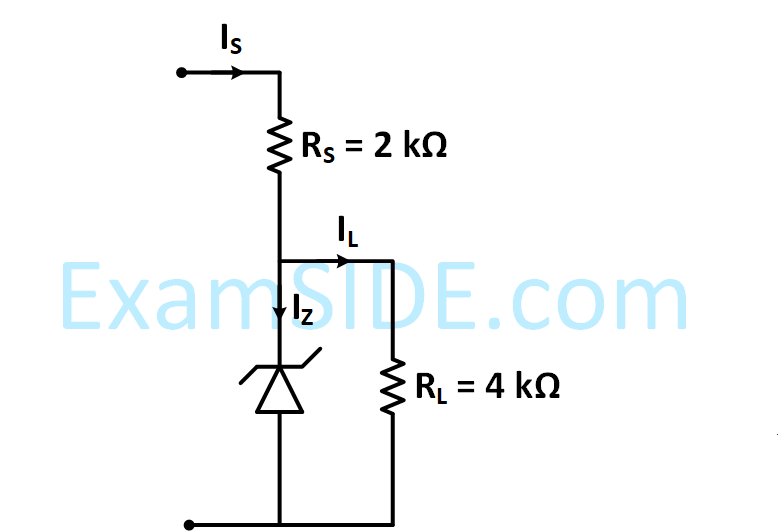
In the given circuit, the value of current IL will be ____________ mA. (When RL = 1k$$\Omega$$)

A transistor is used in common-emitter mode in an amplifier circuit. When a signal of 10 mV is added to the base-emitter voltage, the base current changes by 10 $$\mu$$A and the collector current changes by 1.5 mA. The load resistance is 5 k$$\Omega$$. The voltage gain of the transistor will be _________.


The estimated current gain from the figure is __________.
The value of x, to the nearest integer, is __________.
The value of x is ____________.


When VCE is 10V and IC = 4.0 mA, then value of $$\beta $$ac is __________.