1
GATE ECE 2007
MCQ (Single Correct Answer)
+1
-0.3
In a p+n junction diode under reverse bias, the magnitude of electric field is
maximum at
2
GATE ECE 2007
MCQ (Single Correct Answer)
+1
-0.3
For the function $${e^{ - x}},$$ the linear approximation around $$x=2$$ is
3
GATE ECE 2007
MCQ (Single Correct Answer)
+2
-0.6
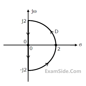
If the semi-circular contour D of radius 2 is as shown in the figure, then the value
of the integral $$\oint\limits_D {{1 \over {{s^2} - 1}}} ds$$ is
4
GATE ECE 2007
MCQ (Single Correct Answer)
+1
-0.3
The equation $${x^3} - {x^2} + 4x - 4 = 0\,\,$$ is to be solved using the Newton - Raphson method. If $$x=2$$ taken as the initial approximation of the solution then the next approximation using this method, will be
Paper Analysis
Total Questions
Analog Circuits 6
Communications 11
Control Systems 11
Digital Circuits 9
Electromagnetics 8
Electronic Devices and VLSI 4
Engineering Mathematics 11
Microprocessors 2
Network Theory 6
Signals and Systems 7
More Papers of GATE ECE
GATE ECE 2026 GATE ECE 2025 GATE ECE 2024 GATE ECE 2023 GATE ECE 2022 GATE ECE 2021 GATE ECE 2020 GATE ECE 2019 GATE ECE 2018 GATE ECE 2017 Set 2 GATE ECE 2017 Set 1 GATE ECE 2016 Set 2 GATE ECE 2016 Set 1 GATE ECE 2016 Set 3 GATE ECE 2015 Set 3 GATE ECE 2015 Set 2 GATE ECE 2015 Set 1 GATE ECE 2014 Set 1 GATE ECE 2014 Set 4 GATE ECE 2014 Set 2 GATE ECE 2014 Set 3 GATE ECE 2013 GATE ECE 2012 GATE ECE 2011 GATE ECE 2010 GATE ECE 2009 GATE ECE 2008 GATE ECE 2007 GATE ECE 2006 GATE ECE 2005 GATE ECE 2004 GATE ECE 2003 GATE ECE 2002 GATE ECE 2001 GATE ECE 2000 GATE ECE 1999 GATE ECE 1998 GATE ECE 1997 GATE ECE 1996 GATE ECE 1995 GATE ECE 1994 GATE ECE 1993 GATE ECE 1992 GATE ECE 1991 GATE ECE 1990 GATE ECE 1989 GATE ECE 1988 GATE ECE 1987
GATE ECE Papers
All year-wise previous year question papers
2026
2025
2024
2023
2022
2021
2020
2019
2018
2013
2012
2011
2010
2009
2008
2007
2006
2005
2004
2003
2002
2001
2000
1999
1998
1997
1996
1995
1994
1993
1992
1991
1990
1989
1988
1987