GATE ECE

Under the DC conditions, the collector-to emitter voltage drop is

In the figure shown above, the OP-AMP is supplied with $$ \pm $$ 15V.
 If the unregulated voltage increases by 20% the power dissipation across the transistor Q$$_1$$
The power dissipation across the transistor Q1 shown in the figure is
If the unregulated voltage increases by 20% the power dissipation across the transistor Q$$_1$$
The power dissipation across the transistor Q1 shown in the figure is
If $${\beta _{DC}}$$ is increased by 10%, the collector-to emitter voltage drop
(i)VGS = 0 at Id = 12 mA and
(ii)VGS = -6 Volts at Zo =$$\infty $$
Which of the following Q-points will give the highest transconductance gain for small signals?
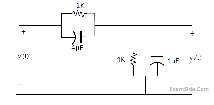
The small-signal gain of the amplifier $${{{V_c}} \over {{V_s}}}$$ is
It is desired to generate a stochastic process (as voltage process) with power spectral density
$$$S\left( \omega \right) = {{16} \over {16 + {\omega ^2}}}$$$By driving a Linear-Time-Invariant system by zero mean white noise (as voltage process) with power spectral density being constant equal to 1. The system which can perform the desired task could be
The parameters of the system obtained in Q. 12 would be
The impulse response of filter matched to the signal $$s(t) = g(t)$$ $$ - \delta {\left( {t - 2} \right)^ * }\,\,g\left( t \right)$$ is given as:
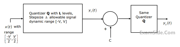
x(t) = 125t(u(t) - u (t - 1) + (250 - 125t) (u (t - 1) - u (t - 2 )) so that slope - overload is avoided, would be
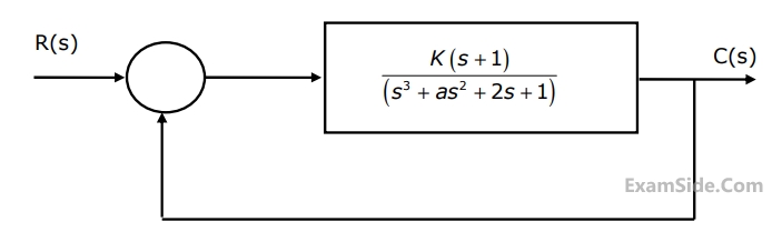
where T > 0. The maximum phase-shift provided by such a compesator is
With the value of "a" set for phase-margin of $$\pi $$/4, the value of unit-impulse response of the open-loop system at t = 1 second is equal to
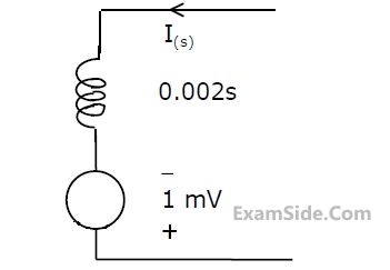
The state-transition matrix of the system is
The inputs D0 and D1 respectively should be connected as


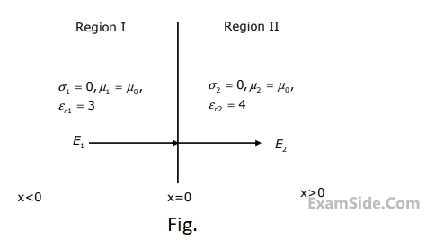
In the figure shown above, the ground has been shown by the symbol $$\nabla $$


The wave is
(i) VGS = 0 at ID = 12 mA and
(ii) VGS = - 6 Volts at ID = 0
Which of the following Q-points will give the highest trans-conductance gain for small signals?
$$F\left( s \right) = {{{\omega _0}} \over {{s^2} + \omega _0^2}},\,\,{\mathop{\rm Re}\nolimits} \left( s \right) > 0.$$ The final value of $$f(t)$$ would be ____________.
(i) $$y=0$$ for $$x=0$$ and
(ii) $$y=0$$ for $$x=a$$
The form of non-zero solution of $$y$$ (where $$m$$ varies over all integrals ) are
Eigen value
$${\lambda _1} = 8$$
$${\lambda _2} = 4$$
Eigen vector
$${V_1} = \left[ {\matrix{
1 \cr
1 \cr
} } \right]$$
$${V_2} = \left[ {\matrix{
1 \cr
-1 \cr
} } \right]$$
The matrix is
LXI SP, EFFF H
CALL 3000 H
3000H: LXI H, 3CF4H
PUSH PSW
SPHL
POP PSW
RET
On completion of RET execution, the contents of SP is

A two-port network is represented by ABCD parameters given by
$$\left[ {\matrix{ {{V_1}} \cr {{I_1}} \cr } } \right] = \,\left[ {\matrix{ A & B \cr C & D \cr } } \right]\,\left[ {\matrix{ {{V_2}} \cr { - \,{I_2}} \cr } } \right]$$
If port-2 is terminated by $${R_L}$$, the input impedance seen at port-1 is given by

The resulting signal is then passed through an ideal low pass filter with bandwidth 1 kHz. The output of the low pass filter would be
would be
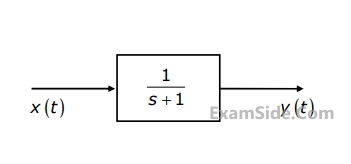
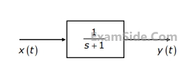
x(t) = (sint)u(t). In steady-state, the response y(t) will be
The final value of f(t) would be: