GATE ECE

(b)Calculate the voltage gain (V0/Vi), of the amplifier with no feedback (Rf=$$\infty $$).
(c)Determine the value of the resistance Rf, required to give a voltage gain (V0/Vi), or - 10.

(a) Draw the impulse response of the matched filter labeling all important points and the axes.
(b) Find the signal shape at the filter output. Lable all important points and axes.

(a)Determine the transfer function and the characteristic equation of the system.
(b)Given that K > 0, find the range of '$$\tau $$' for which the system is unconditionally stable.
(a) Determine G(s), if it is known that the system is of minimum phase type.
(b) Estimate the phase at each of the corner frequencies.


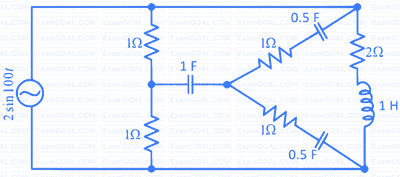
In the signal flow graph shown in fig X2= TX1 where T is equal to


$${V_{OH}}$$ is the minimum output high-level voltage
$${V_{OL}}$$ is the minimum output low-level voltage
$${V_{IH}}$$ is the minimum output high-level voltage and
$${V_{IL}}$$ is the minimum output low-level voltage.
The correct relationship is:
Standard TTL (74XX), Low power TTL(74LXX) Low power schottky TTL(74LSXX), schottky TTL(74 SXXX), Emitter coupled Logic (ECL), CMOS
(a) Among the TTL Families, ________ family requires considerably less power than the standard TTL (74XX) and also has com parable proparation delay.
(b) Only the _______ family can operate over a wide range of power supply voltages.
For M=1, sequence of Q1, Q0 is ..00, 01, 10, 11, 00, 01.......
For M=0, sequence of Q1, Q0 is ..00, 11, 10, 01, 00, 11......
(a)Design the necessary feedback logic for T1 and T0.
(b)Realize the feesback logic using inverters and 4-input multiplexers only. Use Q1 and Q0 as the control inputs of the multiplexer with Q1 as the MSB.


(a) Draw the Karnaugh maps for $${D_1}$$ and $${D_0}$$ in terms of $${C_2}$$, $${C_1}$$ and $${C_0}$$
(b) Obtain the minimal sum of products expressions for $${D_1}$$ and $${D_0}$$.
(c) Realize the logic for $${D_1}$$ and $${D_0}$$ using 2- input NAND gates only.
(d) Find the resolution of the Ato D converter.

(a) Determine the associated magnetic field.
(b) What type of wave does the above field represent?
(i) radiation resistance and
(ii) terminal resistance
(a) the values of $$R$$ and $$C$$
(b) the quality factor of the circuit
A square waveform as shown in the figure is applied across 1 mH ideal inductor.The current through the inductor is a triangular wave of ................. peak amplitude.
