GATE ECE
when $${R_a}\, = \,{R_b}\, = \,{R_c}\,{R_d}\,$$ ohms.
when $${R_a}\, = \,{R_b}\, = {R_c}\, = 100$$ ohms and $${R_{d\,}}\, = \,120$$ ohms.


(a) In absence of derivative feedback (Kt=0) , determine damping ratio of the system for amplifier gain KA=5. Also find the steady state error to unit ramp input.
(b) Find suitable values of the parameters KA and Kt so that damping ratio of the system is increased to 0.7 without affecting the steady state error as obtained in part (a).

Sketch Nyquist plot for the system and there from obtain the gain margin and the phase margin.


A is false and B is true
A is false and C is true
A, B and C are all false
A, B and C are all true.
(a)Write the truth table for F. use the convention, true = 1 and false = 0.
(b)Write the simplified expression for F as a Sum of Products.
(c) Write the simplified expression for F as a product of Sums.
(d) Draw a logic circuit implementation of F using the minimum number of 2
input NAND gates only.
If XY=00, the flip-flop changes stage with each clock pulse.
If XY=01, the flip-flop state Q becomes 1 with the next clock pulse.
If XY=10, the flip-flop state Q becomes 0 with the next clock pulse.
If XY=11, no change of state occurs with the clock pulse.
(a) Write the Truth table for the X-Y flip flop
(b) Write the Excitation table for the X-Y flip flop
(c) It is desired to convert a J-K flip flop into the X-Y flip flop by adding some external gates, if necessary. Draw a circuit to show how you will implement the X-Y flip-flop using a J-K flip-flop.

Calculate the power per square metre that causes heating of the brass sheet, taking $${ \in _r} = 1,\,\,\,{\mu _r} = 1$$ and $$\sigma = 1.649 \times {10^7}\,\,\,\,\,$$ mhos/metre for brass.


 At the completion of execution of the program, the program Counter of the 8085 contains ________ and the Stack Pointer contains ________.
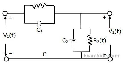
For the compensated attenuator of figure, the impulse response under the condition $$R_1C_1\;=\;R_2C_2$$ is:

Of the four networks, N1,N2, N3 and N4 of figure, the networks having identical driving point functions are

For the circuit shown below different time constants are given :

1. $0.5 \times 10^{-3} \mathrm{sec}$
2. $2 \times 10^{-3} \mathrm{sec}$
3. $0.25 \times 10^{-3} \mathrm{sec}$
4. $10^{-3} \mathrm{sec}$
What are the charging and discharging times respectively :
Assuming that x(t) is ideally sampled at a sampling frequency of 3 kHz, sketch
(i) x(f), and
(ii) the spectrum of the sampled signal for $${\,\left| f \right|\, \le \,\,3\,kHz}$$.