GATE ECE

Transistor data gm = 5mA/V, $${r_\pi }\, = \,200K\Omega, $$ $${C_\pi }\, = \,1.5$$ pF and $$C\mu \, = \,0.5$$ pF determine the upper cutoff frequency fH of the amplifier
$$g\matrix{ c \cr m \cr } \left[ { \buildrel \Delta \over = {{{i_c}^c} \over {{v_{be}}^c}}} \right]$$ is given by

Group - I
(a)Cascode amplifier(b)Differential Amplifier
(c)Darlington pair common-collector Amplifier
Group - II
(1)does not provide current gain(2)is a wide band Amplifier
(3)has very low input impedance Emitter Amplifier and very high current gain
(4)has very high input impedance and very high current gain
(5)Provides high common mode voltage Rejection


(a) Express F in the minimum sum-of-products from.
(b) Express F in the minimum product-of-sums from.
(c) Assuming that both true and complement froms of the input variables are avialable, draw a cicruit to implement F using the minimum number of 2input NAND gates only.
By using an OR gate array as shown in figure where $${P_{1\,}}\,to\,{P_5}$$ are the product terms in one or more of the variables a, $$\overline a $$, b, $$\,\overline b $$, c and $$\overline c $$.


(a) Write the 4-bit values (Q0Q1Q2Q3) after each clock pulse till the pattern (1000) reappears on (Q0Q1Q2Q3).
(b) To what values should the shift register be intialized so that the pattern (1001) occurs after the first clock pulse?

One possible implementation of the state machine is shown figure. Specify what signals should be applied to each of the multiplexer inputs

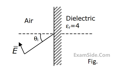
(i) The angle of incidence $${\theta _i}$$ for which there is no reflection of the wave.
(ii) The surface charge density at the interface.
Find the vector magnetic field and the phase velocity of the wave inside the waveguide.

1000: LXI SP< 27FF
1003: CALL 1006
1006: POP H
The contents of the stack pointer (SP) and the HL register pair on completion or execution of these instructions are.

Write down the short circuit admittance matrix $${{Y_{SC}}}$$ of the network viewed as a two-port network, but now taking B as the input terminal, C as the output terminal and A as the common terminal.
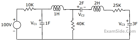
The voltage VC1, VC2 and VC3 across the capacitors in the circuit in Fig., under steady state, are respectively
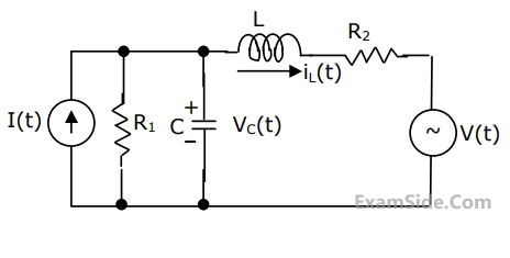 Choosing the voltage vC(t) across capacitor, and the current iL(t) through the inductor as state variable,i.e.,
$$$\left[\mathrm x\left(\mathrm t\right)\right]\;=\;\begin{bmatrix}{\mathrm v}_\mathrm C\left(\mathrm t\right)\\{\mathrm i}_\mathrm L\left(\mathrm t\right)\end{bmatrix}$$$
Write the state equation in the form $$\frac{\operatorname d\left[x\left(t\right)\right]}{\operatorname dt}\;=\;\left[A\right]\left[x\left(t\right)\right]\;+\;\left[B\right]\left[u\left(t\right)\right]$$ and find [A], [B] and [u(t)].
Choosing the voltage vC(t) across capacitor, and the current iL(t) through the inductor as state variable,i.e.,
$$$\left[\mathrm x\left(\mathrm t\right)\right]\;=\;\begin{bmatrix}{\mathrm v}_\mathrm C\left(\mathrm t\right)\\{\mathrm i}_\mathrm L\left(\mathrm t\right)\end{bmatrix}$$$
Write the state equation in the form $$\frac{\operatorname d\left[x\left(t\right)\right]}{\operatorname dt}\;=\;\left[A\right]\left[x\left(t\right)\right]\;+\;\left[B\right]\left[u\left(t\right)\right]$$ and find [A], [B] and [u(t)].Match each of the items of Set 1, with the appropriate item of the Set 2.

Set 2
(1) current increases monotonically with time
(2) current decreases monotonically with time
(3) current remains constant at V/R
(4) current first increases, then decreases
(5) no current can ever flow
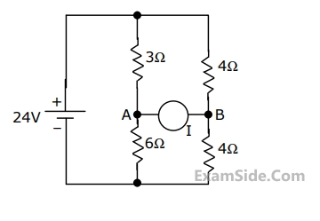
In the circuit shown in Fig., it is known that the variable current source I absorbs power.Find I (in magnitude and direction) so that it receives maximum power and also find the amount of power absorbed by it.