GATE ECE
c(t) and m(t) are used to generate an FM signal. If the peak frequency deviation of the generated FM signal is three times the transmission bandwidth of the AM singal, then the coefficient of the term $$\cos\left[2\mathrm\pi\left(1008\times10^3\right)t\right]$$ in the FM signal (in terms of the Bessel coefficients) is
c(t) and m(t) are used to generate an AM signal. The modulation index of the generated AM signal is 0.5. Then the quantity $$\frac{Total\;sideband\;power}{Carrier\;power}$$ is

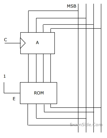
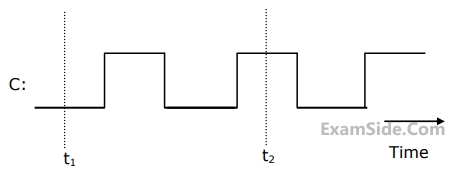
The clock to the register is shown, and the data on the W bus at time t$$_1$$ is 0110. The data on the bus at time t$$_2$$ is
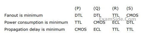
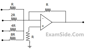 The input bits 0 and 1 are represented by 0 and 5 V respectively. The OP- AMP is ideal, but all the resistances and the 5V inputs have a tolerance of ±10%.
The specification (rounded to the nearest multiple of 5%) for the tolerance of the DAC is
Y = $$\,P \oplus \,Q\, \oplus \,R$$
z= $$RQ + \overline P R\, + Q\,\overline P $$
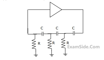
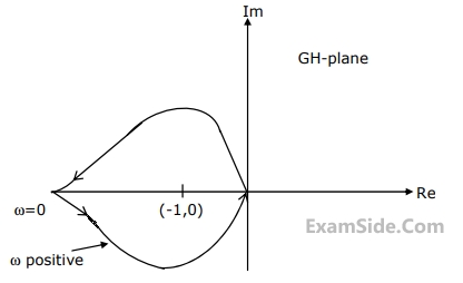
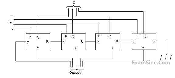 The circuit acts as a
W= R+$$\overline P Q + \overline R $$ S
X = $$X = PQ\overline R \,\overline S + \overline P \,\overline Q \,\overline R \,\overline S + P\overline Q \,\overline R \,\overline S $$
Y = $$RS + \overline {OR + P\overline Q + \overline {PQ} } $$
Z = $$R + S + \overline {PQ + \overline {PQR} + P\overline {QS} } $$
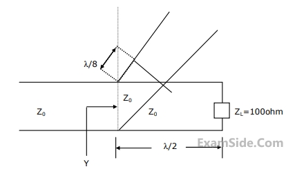
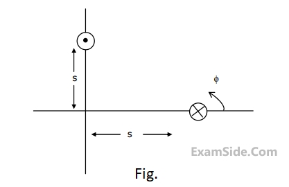
$$E\left( {z,\,t} \right) = \,10\,\cos \left( {2\pi \times {{10}^7}\,\,t - 0.1\,\,\pi z} \right)\,$$ volt/m, the velocity of the traveling wave is
$$I\left( s \right) = {2 \over {s\left( {1 + s} \right)}}$$ As $$t \to \infty ,$$ the value of $$i(t)$$ tends to __________.

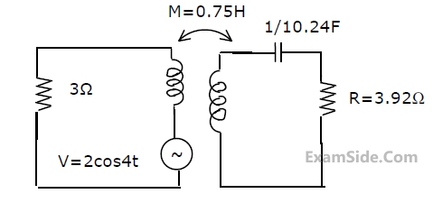

The circuit is given in figure.Assume that the switch S is in position 1 for a long time and thrown to position 2 at t = 0.
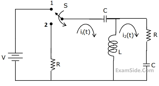
I1(s) and I2(s) are the Laplace transforms of i1(t) and i2(t) respectively. The equations for the loop currents I1(s) and I2(s) for the circuit shown in figure, after the switch is brought from position 1 to position 2 at t = 0, are
The circuit is given in figure.Assume that the switch S is in position 1 for a long time and thrown to position 2 at t = 0.
At t = 0+, the current i1 is
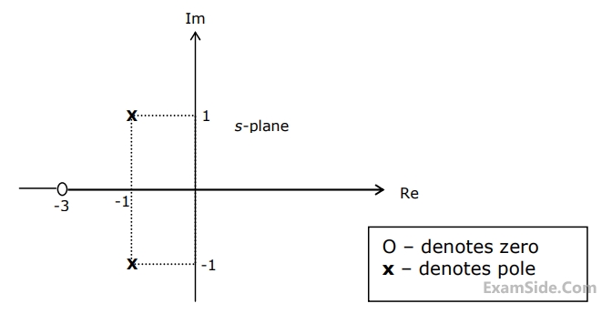
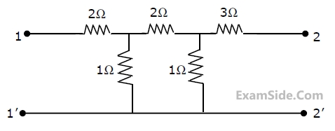
Twelve 1Ω resistances are used as edges to form a cube. The resistance between two diagonally opposite corners of the cube is
where $$\matrix{ {\delta \left( n \right) = 1,} & {n = 0} \cr {0,} & {otherwise} \cr } $$
The output at $$n = 4$$ is
$$I\left( s \right)\,\, = \,{2 \over {s\left( {1 + s} \right)}}$$
As $$t \to \infty $$ , the value of i(t) tends to
Let $${t_g}$$ (f) be the group delay function of the given RC-LPF and $${f_2}$$ = 100 Hz. Then $${t_g}$$$${(f_2)}$$ in ms, is
Let H(t) denote the frequency response of the RC-LPF. Let $${f_1}$$ be the highest frequency such that $$0 \le \left| f \right| \le {f_1},{{\left| {H({f_1})} \right|} \over {H(0)}} \ge 0.95$$. Then $${f_1}$$ (in Hz) is
A discrete time system has the input-output relationship,
$$y\left( n \right) = \left\{ {\matrix{ {x\left( n \right),} & {n \ge 1} \cr {0,} & {n = 0} \cr {x\left( {n + 1} \right),} & {n \le - 1} \cr } } \right.$$
Where $$x\left( n \right)\,$$ is the input and $$y\left( n \right)\,$$ is the output. The above system has the properties