1
MHT CET 2025 5th May Evening Shift
MCQ (Single Correct Answer)
+1
-0
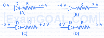
Which of the following figure represents forward bias diode?
2
MHT CET 2025 5th May Evening Shift
MCQ (Single Correct Answer)
+1
-0
An AND gate is followed by a NOT gate in series. With two inputs ' $A$ ' and ' $B$ ', the Boolean expression for the output ' Y ' will be
3
MHT CET 2025 26th April Evening Shift
MCQ (Single Correct Answer)
+1
-0
If p-n junction diode is forward biased, then
4
MHT CET 2025 26th April Evening Shift
MCQ (Single Correct Answer)
+1
-0
In a certain 2 -inputs logic gate, when inputs $\mathrm{A}=0$ and $\mathrm{B}=0$, then output $\mathrm{C}=1$. And also when inputs $\mathrm{A}=0, \mathrm{~B}=1$, then again output $\mathrm{C}=1$. The gate must be
MHT CET Subjects
Browse all chapters by subject
Chemistry
Physical Chemistry
Some Basic Concepts of Chemistry Atomic Structure States of Matter Thermodynamics Chemical Equilibrium Ionic Equilibrium Liquid Solution Redox Reactions Surface Chemistry Solid State Electrochemistry Chemical Kinetics Nuclear Chemistry
Inorganic Chemistry
Periodic Table and Periodicity Chemical Bonding and Molecular Structure Metallurgy Hydrogen and It's Compounds s-Block Elements p-Block Elements d and f Block Elements Coordination Compounds Environmental Chemistry
Organic Chemistry
Mathematics
Algebra
Sets and Relations Logarithms Quadratic Equations Sequences and Series Binomial Theorem Permutations and Combinations Probability Vector Algebra Three Dimensional Geometry Matrices and Determinants Statistics Mathematical Reasoning Linear Programming Complex Numbers
Trigonometry
Trigonometric Ratios & Identities Trigonometric Equations Inverse Trigonometric Functions Properties of Triangles
Calculus
Functions Limits, Continuity and Differentiability Differentiation Application of Derivatives Indefinite Integration Definite Integration Area Under The Curves Differential Equations
Coordinate Geometry
Physics
Mechanics
Units & Measurement and Dimensions Vector Algebra Motion Laws of Motion Circular Motion Work, Energy and Power Center of Mass and Collision Rotational Motion Gravitation Simple Harmonic Motion Fluid Mechanics Elasticity Waves Heat and Thermodynamics
Optics
Electromagnetism
Electrostatics Current Electricity Capacitor Moving Charges and Magnetism Magnetism and Matter Electromagnetic Waves Electromagnetic Induction Alternating Current
Modern Physics