Semiconductor Devices and Logic Gates · Physics · MHT CET
MCQ (Single Correct Answer)
When LED is manufactured by using aluminium gallium arsenide (AlGaAs), it emits
Which of the following figure represents forward bias diode?

An AND gate is followed by a NOT gate in series. With two inputs ' $A$ ' and ' $B$ ', the Boolean expression for the output ' Y ' will be
If p-n junction diode is forward biased, then
In a certain 2 -inputs logic gate, when inputs $\mathrm{A}=0$ and $\mathrm{B}=0$, then output $\mathrm{C}=1$. And also when inputs $\mathrm{A}=0, \mathrm{~B}=1$, then again output $\mathrm{C}=1$. The gate must be
For a transistor, $\alpha_{\mathrm{dc}}$ and $\beta_{\mathrm{dc}}$ are the current ratios, then the value of $\frac{\beta_{\mathrm{dc}}-\alpha_{\mathrm{dc}}}{\alpha_{\mathrm{dc}} \times \beta_{\mathrm{dc}}}$
In a common emitter transistor amplifier circuit, the input resistance is $1.8 \mathrm{k} \Omega$ and output is obtained across a load resistance of $9 \mathrm{k} \Omega$. The alternating current gain is 70 . Corresponding to an a.c. input voltage of 6 mV , the output voltage will be
Applying forward bias to p-n junction, the potential barrier
The material used for solar cell should have band gap
One of the following values of inputs $\mathrm{A}, \mathrm{B}$ and C respectively gives output $(\mathrm{Y})$ of the following combination of logic gates as ' 1 ' is

A piece of semiconductor is connected in series in an electric circuit. On increasing the temperature, the current in the circuit will
In a common emitter amplifier configuration, the current gain is 62 . The collector resistance and input resistance are $5 \mathrm{k} \Omega$ and $500 \Omega$ respectively. If the input voltage is 0.01 V , the output voltage will be
The logic gate for which the output goes 'HIGH' or ' 1 ' only when an odd number of 'HIGH' or ' 1 ' are at its input, is
To get output of the following logic circuit as ' 0 ' (zero), the inputs $A, B, C$ should NOT be, respectively,

In which of the following figures, the p.n. junction diode is reverse biased?


I - V characteristics of photodiode for different illumination intensities $\mathrm{I}_1, \mathrm{I}_2, \mathrm{I}_3$ and $\mathrm{I}_4$ are drawn as follows. Then the maximum intensity among them is

$\mathrm{I}-\mathrm{V}$ characteristics of LED is shown correctly by graph
By increasing the temperature, the specific resistance of a conductor and a semiconductor respectively
Which of the following statements is TRUE for n-type semiconductor?
In a common emitter transistor amplifier circuit, the current gain $\alpha=0.8$. If the base current changes by $3 \mu \mathrm{~A}$ then the collector current changes by
In the case of common emitter transistor amplifier, the ratio of collector current to emitter current is 0.96 , then the current gain $(\beta)$ of the amplifier is
In the logic circuit given, $\mathrm{A}, \mathrm{B}$ and C are the inputs and Y is the output. The output Y is HIGH

The graph given below represents I-V characteristics of zener diode. The part of the characteristics curve that is most relevant for its operation as a voltage regulator is

In n-type semiconductor, free electrons donated by the impurity atoms occupy energy levels in
In a pure silicon crystal electron-hole concentration is $10^{16}$ per $\mathrm{m}^3$ at 301 K . Now $10^{21}$ atoms of phosphorus are added per cubic metre. The new hole concentration in silicon is (in per $\mathrm{m}^3$ )
In a common emitter transistor amplifier, the output voltage and input voltage have a phase difference of
If a centre tap transformer is used with two p-n junction diodes for full wave rectification then output voltage of rectifier with respect to each diode is (secondary voltage of transformer $=\mathrm{V}_{\mathrm{s}}$ )
If an alternating voltage is applied across a p-n junction diode in series with a load then
In the following combination of logic gates, the output $Y$ can be written in the terms of inputs $A$ and B as

In common emitter mode of a transistor, the current gain is 8 . The input impedance is $25 \mathrm{k} \Omega$ and load resistance is $75 \mathrm{k} \Omega$. The power gain is
If the internal resistance of cell is negligible then current flowing through the circuit is
Which of the following logic gates is called as Universal gate?
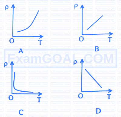
Which graph shows correctly the temperature (T). dependence of resistivity $(\rho)$ of a semiconductor?
In an n-p-n transistor amplifier, the collector current is 8 mA . If $80 \%$ of the electrons from the emitter reach the collector, then ( $\alpha$ and $\beta$ are current ratios)
In an n-p-n transistor amplifier, the collector current is 9 mA . If $90 \%$ of the electrons emitted reach the collector, then
The resultant logic gate from the combination of following gates is

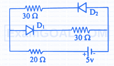
In the following circuit shown in figure, three diodes are connected each with forward resistance $40 \Omega$ and infinite backward resistance. The current through $100 \Omega$ resistance is
For an ideal diode, in forward and reverse biased condition the resistance is respectively
When an n-p-n junction transistor is used as an amplifier in common emitter mode,
In a transistor (common emitter configuration) the ratio of power gain to voltage gain is ( $\alpha$ and $\beta$ are current ratios)
In a given logic circuit, the output Y when all the three inputs $\mathrm{A}, \mathrm{B}, \mathrm{C}$ are first low and then high will be respectively

In unbiased p-n junction diode
In a transistor amplifier, AC current gain is 64 , the load resistance is $5400 \Omega$ and the input resistance of the transistor is $540 \Omega$. The voltage gain is
To get the truth table shown from the following logic circuit, the logic gate G should be

The Boolean expression for the given combination of logic gates is

When a small amount of impurity atoms are added to semiconductor, then generally its resistivity
The input signal given to C.E. amplifier having a voltage gain of 126 is $V_i=2 \cos \left(12 t+\frac{\pi}{3}\right)$. The corresponding output signal will be
The truth table of the following circuit is

If the $\mathrm{p}-\mathrm{n}$ junction diode is unbiased,
For detecting light intensity we use
What is the current in the following junction diode circuit?

A p-n junction diode as a rectifier converts
Two different logic gates giving output ' 1 ' for the inputs $(1,0)$ and then for $(0,1)$ are
In an extrinsic n-type semiconductor, the free electrons donated by the impurity atoms occupy energy levels in
For a transistor, current gain $(\beta)=50$. To change the collector current by $350 \mu \mathrm{~A}$, the base current should be changed by
When n-p-n junction transistor is used as an amplifier in common emitter mode,
Assuming that junction diode is ideal, the current in arrangement shown in figure

For the following digital logic circuit, the correct truth-table is

Following combination of gates is equivalent to

If ' $\mathrm{n}_{\mathrm{c}}$ ' and ' $\mathrm{n}_{\mathrm{h}}$ ' are the number of electrons and number of holes respectively in a semiconductor heavily doped with phosphorous then
A p-n junction diode cannot be used
In semiconductors at room temperature,
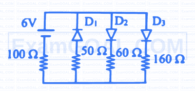
In the given circuit, Zener breakdown voltage is 8 V . If power of Zener diode is 1.6 W . The value of $R$ is

The logic gate represented by following logic circuit is

Two ideal diodes are connected to a battery as shown in the circuit. The current supplied by the battery is

What is the output Y in the following circuit, when all the three inputs A, B, C are first 'zero' and then 'one'?

In the block diagram of simple rectifier circuit, from a variable a.c. voltage, constant d.c. voltage is obtained. The correct order of operation is
In the working of photodiode, the reverse current depends on
The resultant gate and its Boolean expression in the given circuit is

The current amplification factor of a transistor is 50 . The input resistance when used in common emitter mode is $1 \mathrm{k} \Omega$. The peak value for an a.c. input voltage of 0.01 V peak is
In the logic circuit diagram, when all the four inputs $\mathrm{A}, \mathrm{B}, \mathrm{C}, \mathrm{D}$ are one, the outputs $\mathrm{Y}_1, \mathrm{Y}_2, \mathrm{Y}_3$ are respectively $(1,1,0)$. When all the inputs $\mathrm{A}, \mathrm{B}, \mathrm{C}, \mathrm{D}$ are changed to 'zero', the outputs $\mathrm{Y}_1, \mathrm{Y}_2, \mathrm{Y}_3$ respectively change to

For the diagram shown, the resistance between points A and B when the ideal diode ' $D$ ' is forward biased is ' $R_1$ ' and that when reverse biased is ' $R_2$ '. The ratio $\frac{R_1}{R_2}$ is

The truth table for the given logic circuit is

In the circuit diagram shown in figure, the current through the zener diode is

The depletion layer in p-n junction region is caused by
The collector supply voltage is 6 V and a voltage drop across a resistor of $600 \Omega$ in the collector circuit is 0.6 V , in a circuit of transistor connected in common emitter mode. If the current gain is 20 then the base current is
A zener diode, having breakdown voltage 15 V is used in a voltage regulator circuit as shown. The current through the zener diode is

A semiconductor device X is connected in series with a battery and a resistor. The current of 10 mA is found to pass through the circuit. If the terminals of X are connected in reverse manner, the current drops to almost zero. X may be
The Boolean expression for ' $x-O R$ ' gate $C=(A \oplus B)$ is equal to
Which one of the following statements is true? A p-type semiconductor is doped with
The combination of NAND gates is shown in figure (I) and (II). For the given inputs, the outputs in both the combinations are respectively.

An n-p-n transistor can be considered to be equivalent to two diodes connected. The correct figure out of the following is

Find the magnitude of current in the given circuit.

In common emitter transistor amplifier, load resistance is $6.5 \mathrm{k} \Omega$ and an input resistance is $1.3 \mathrm{k} \Omega$. If the current gain is 78 , the voltage gain is
The potential barrier in p-n junction diode is due to
The logic gate combination circuit shown in the figure performs the logic function of

In semiconductors at room temperature,
The logic circuit in figure is equivalent to

In an NPN transistor $10^{10}$ electrons enter the emitter in $10^{-6} \mathrm{~s}$ and $2 \%$ electrons recombine with holes in base. The current ratios ' $\alpha$ ' and ' $\beta$ ' of a transistor are respectively (nearly)
The output of following combination is same as that of

In an n-p-n transistor, the collector current is $$28 \mathrm{~mA}$$. If $$80 \%$$ of electrons reach the collector, its base current in $$\mathrm{mA}$$ is
When the conductivity of a semiconductor is only due to the breaking of the covalent bonds, the semiconductor is called
For a common emitter configuration, if '$$\alpha$$' and '$$\beta$$' have their usual meanings, the incorrect relation between '$$\alpha$$' and '$$\beta$$' is
For emission of light, a light emitting diode (LED) is
In semiconductors at room temperature,
The Boolean expression for the following combination is

If the maximum efficiency of a full wave rectifier is $$x \%$$ and that of half-wave rectifier is $$y \%$$, then the relation between $$x$$ and $$y$$ is
Doping of a semiconductor (with small impurity atoms) generally changes the resistivity as follows.
The following graph represents

If two inputs of a NAND gate are shorted, the resulting gate is
On increasing the reverse bias to a large value in a P-N junction diode, current
In the following digital logic circuit, the output Y will be '1' for inputs

Which one of the following statements is WRONG regarding LED?
In which figure, the junction diode is forward biased?
The following logic gate combination is equivalent to

The logic gate combination circuit shown in the figure performs the logic function of

When forward bias is applied to a p-n junction, then what happens to the potential barrier $$\left(V_B\right)$$ and the width $$(\mathrm{X})$$ of the depletion region?
In the study of transistor as an amplifier if $$\alpha=\frac{I_C}{I_E}=0.98$$ and $$\beta=\frac{I_C}{I_B}=49$$, where $$I_C, I_B$$ and $$\mathrm{I}_{\mathrm{E}}$$ are collector, base and emitter current respectively then $$\left(\frac{1}{\alpha}-\frac{1}{\beta}\right)$$ is equal to
If $$p$$-$$n$$ junction diode is in forward bias then
In the digital circuit the inputs are as shown in figure. The Boolean expression for output $$\mathrm{Y}$$ is

Identify the correct circuit diagrams for the normal operation from the following.

In energy band diagram of insulators, a band gap and the conduction band is respectively
In the case of NAND gate, if A and B are the inputs and $$\mathrm{Y}$$ is the output then
A pure $$\mathrm{Si}$$ crystal has $$4 \times 10^{28}$$ atoms per $$\mathrm{m}^3$$. It is doped by 1 ppm concentration of antimony. The number of free electrons available will be
The output of an 'OR' gate is connected to both the inputs of a 'NAND' gate. The combination will serve as
Which one of the operations of $$\mathrm{n}-\mathrm{p}-\mathrm{n}$$ transistor differs from that of $$p-n-p$$ transistor?
For the diagram shown, the resistances between points A and B when ideal diode D is forward biased is '$$R_1$$' and that when reverse biased is '$$R_2$$'. The ratio $$R_1: R_2$$ is

To obtain the truth-table shown, from the following logic circuit, the gate G should be

In insulators
Identify the mismatch out of the following.
In the reverse biasing of a p-n junction diode :
In a transistor, in common emitter configuration, the ratio of power gain to voltage gain is
If the frequency of the input voltage is $$50 \mathrm{~Hz}$$, applied to a (a) half wave rectifier and (b) full wave rectifier. The output frequency in both cases is respectively
For an intrinsic semiconductor $$\left(\mathrm{n}_{\mathrm{h}}\right.$$ and $$\mathrm{n}_{\mathrm{e}}$$ are the number of holes per unit volume and number of electrons per unit volume respectively)
A $$5.0 \mathrm{~V}$$ stabilized power supply is required to be designed using a $$12 \mathrm{~V}$$ DC power supply as input source. The maximum power rating of zener diode is $$2.0 \mathrm{~W}$$. The minimum value of resistance $$R_{\mathrm{s}}$$ in $$\Omega$$ connected in series with zener diode will be
To get the truth table shown, from the following logic circuit, the Gate G should be

For a NAND gate, the inputs and outputs are given below.
| Input A | Input B | Output Y |
|---|---|---|
| 0 | 1 | $$\mathrm{C}$$ |
| 0 | 0 | $$\mathrm{D}$$ |
| 1 | 0 | $$\mathrm{E}$$ |
| 1 | 1 | $$\mathrm{F}$$ |
The values taken by C, D, E, F are respectively
The given circuit has two ideal diodes $$D_1$$ and $$D_2$$ connected as shown in the figure. The current flowing through the resistance $$R_1$$ will be

Choose the correct statement. In conductors
For a transistor, the current ratio $$\alpha_{\mathrm{dc}}=\frac{69}{70}$$, the current gain $$\beta_{\mathrm{dc}}$$ is
The input a.c. voltage of frequency $$60 \mathrm{~Hz}$$ is applied to half-wave rectifier and also to full-wave rectifier. The output frequency in case of half-wave rectifier and that in case of full wave rectifier is respectively.
A p-n junction photodiode is fabricated from a semiconductor with a band gap of $$2.5 \mathrm{~eV}$$. It can detect a signal of wavelength [Planck's constant $$=6.6 \times 10^{-34} \mathrm{Js}, \mathrm{c}=3 \times 10^8 \mathrm{~m} / \mathrm{s}, \mathrm{e}=1.6 \times 10^{-19} \mathrm{C}$$]
For the output of the following logic circuit to be 'I', the values of inputs A and B should be respectively

Two identical ideal diodes are connected to an ammeter and a d.c source (1 volt) as shown. In which one of the following circuits, ammeter will not show any deflection?

When the temperature of a semiconductor is increased, its resistance and electric conductivity respectively.
For a two input AND gate, the four entries are shown in the truth table. Identify the correct ones out of these $$(\mathrm{A}, \mathrm{B}=$$ input, $$\mathrm{Y}=$$ output)
| Entry | A | B | Y |
|---|---|---|---|
| 1 | 0 | 1 | 0 |
| 2 | 1 | 0 | 0 |
| 3 | 1 | 1 | 1 |
| 4 | 0 | 0 | 1 |
In a CE transistor, a change of $$8.0 \mathrm{~mA}$$ in the emitter current produces a change of $$7.8 \mathrm{~mA}$$ in the collector current. What change in the base current is necessary to produce the same change in the collector current?
The resultant gate and its Boolean expression in the given circuit is

What are the values of the currents flowing in each of the following diode circuits $$\mathrm{X}$$ and $$\mathrm{Y}$$ respectively? (Assume that the diodes are ideal)

In common emitter amplifier, a change of 0.2 mA in the base current causes a change of 5 mA in the collector current. If input resistance is 2 k$$\Omega$$ and voltage gain is 75, the load resistance used in the circuit is
Which of the following gates will give an output '1' for the given inputs?

For a common-emitter amplifier, the voltage gain is 40. Its input and output impedances are $$100 \Omega$$ and $$400 \Omega$$, respectively. The power gain of the CE amplifier will be
Choose the correct statement. In semiconductors valance band and conduction band
A logic gate which gives output 'HIGH' only when its two input terminals are at different logic levels with respect to each other is
Choose the FALSE statement from the following.
In an n-p-n transistor 200 electrons enter the emitter in 10$$^{-8}$$ second. If 1% electrons are lost in the base, then the current that enters the emitter and the current amplification factor are respectively [e = 1.6 $$\times$$ 10$$^{-19}$$ C]
Combination of NAND gates is shown in the figure. It is equivalent to

In an ideal junction diode, the current flowing through PQ is

LED is manufactured using zinc selenide then it emits.
In a pure silicon, number of electrons and holes per unit volume are $$1.6 \times 10^{16} \mathrm{~m}^{-3}$$. If silicon is doped with Boron in a way that on doping hole density increases to $$4 \times 10^{22} \mathrm{~m}^{-3}$$. Then electron density in doped semiconductor will be
For a transitor, $$\frac{1}{\alpha_{\mathrm{DC}}}-\frac{1}{\beta_{\mathrm{DC}}}$$ is equal to [ $$\alpha_{\mathrm{DC}}$$ and $$\beta_{\mathrm{DC}}$$ are current amplification factors]
The current in the following circuit is

The output of an 'OR' gate is 'one'
In the case of insulators, a band gap and conduction band is respectively
A rectifier is used to
Two different logic gates moving output '0' for the inputs (0, 1) and then for (1, 0) are
The frequency of a given a.c. signal is 'N' Hz. When it is connected to a half wave rectifier, the number of output pulses given by the rectifier in 1 second is
Silicon and copper are cooled from 300 K to 100 K, the specific resistance (resistivity)
A transistor having $\alpha=0.8$ is connected in common emitter configuration. When the base current changes by 6 mA , then the change in collector current is
In an intrinsic semiconductor, at an ordinary temperature, the correct relation between the number of electrons per unit volume $n_e$ and number of holes per unit volume $n_h$.
$$A$$ transistor has a voltage gain $$A$$. If the amount $$\beta A$$ of its output is applied to the input of the transistor, then the transistor becomes oscillator, when
At absolute zero temperature, pure silicon behaves as
In common emitter amplifier, input resistance is $$1000 \Omega$$, peak value of input signal voltage is $$5 \mathrm{~mV}$$ and $$\beta=60$$. The peak value of output current is
When a small amount of impurity atoms are added to a semiconductor, then generally its resistivity
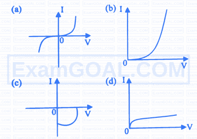
$V-I$ characterstics of LED is shown correctly by graph
Which of the following regions of a transistors are, respectively, heavily dopped and lightly dopped?
In case of $p$-n junction diode, the width of depletion region is
In the study of transistor as an amplifier, the ratio of collector current to emitter current is 0.98 then the ratio of collector current to base current will be
Assuming that the junction diode is ideal, the current in the arrangement shown in figure is

. For a transistor, the current ratio ' $\beta_{d c}$ ' is defined as the ratio of