1
GATE EE 2026
MCQ (Single Correct Answer)
+2
-0
The MOSFET switches shown in the circuit are ideal.
Which of the following is the correct option for Boolean logical expression of the output (OUT), and the maximum possible power (P) consumed by the circuit?
2
GATE EE 2010
MCQ (Single Correct Answer)
+2
-0.6
The $$TTL$$ circuit shown in the figure is fed with the waveform $$X$$ (also shown). All gates have equal propagation delay of $$10$$ $$ns.$$ The output $$Y$$ of the circuit is


A

B

C

D

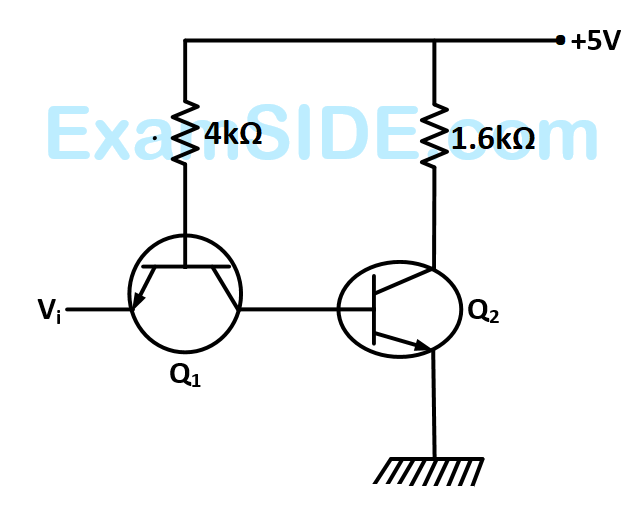
3
GATE EE 2006
MCQ (Single Correct Answer)
+2
-0.6
A TTL NOT gate circuit is shown in figure. Assuming $${V_{BE}} = 0.7\,v$$ of both the transistors, if $${V_i} = 3.0\,V,$$ then the states of the two transistors will be
GATE EE Subjects
Browse all chapters by subject
Electric Circuits
Electrical Machines
Engineering Mathematics
Signals and Systems
Power Electronics
Power System Analysis
Digital Electronics
Analog Electronics
Electromagnetic Fields
Control Systems
Electrical and Electronics Measurement
General Aptitude