Bjt and Mosfet Biasing · Analog Electronics · GATE EE
Marks 1
1
Which one of the following statements is true about the small signal voltage gain of a MOSFET based single stage amplifier?
GATE EE 2025
2
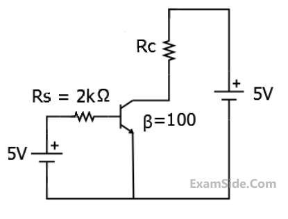
In the BJT circuit shown, beta of the PNP transistor is 100 . Assume $V_{B E}=-0.7 \mathrm{~V}$. The voltage across $R_C$ will be 5 V when $R_2$ is $\_\_\_\_$ $\mathrm{k} \Omega$. (Round off to 2 decimal places)

GATE EE 2021
3
A transistor circuit is given below. The Zener diode breakdown voltage is $$5.3$$ $$V$$ as shown. Take base to emitter voltage drop to be $$0.6$$ V. The value of the current gain $$\beta $$ is ________.

GATE EE 2016 Set 1
4
In the given circuit, the silicon transistor has $$\beta $$ $$=75$$ and a collector voltage $${V_C} = 9\,V.$$ Then the ratio of $${R_B}$$ and $${R_C}$$ is ___________.

GATE EE 2015 Set 1
5
When a bipolar junction transistor is operating in the saturation mode, which one of the following statements is TRUE about the state of its collector-base (CB) and the base-emitter (BE) junctions?
GATE EE 2015 Set 2
6
In the following circuit, the transistor is in active mode and $${V_C} = 2V.$$ To get $${V_C} = 4V,$$ we replace $${R_C}$$ with $${R_C}.$$ Then the ratio $$R{'_C}/{R_C}$$ is __________.

GATE EE 2015 Set 2
7
The transistor in the given circuit should always be in active region. Take $${V_{CE\left( {sat} \right)}} = 0.2\,\,V,\,\,\,{V_{BE}} = 0.7\,\,V.\,\,\,$$ The maximum value of $${R_C}$$ in $$\Omega $$ which can be used, is __________.
GATE EE 2014 Set 2
8
The magnitude of the mid-band voltage gain of the circuit shown in figure is (assuming $${h_{fe}}$$ of the transistor to be $$100$$)

GATE EE 2014 Set 1
9
The three terminal linear voltage regular is connected to a $$10\Omega $$ load resistor as shown in the figure. If $${V_{in}}$$ is $$10$$ $$V,$$ what is the power dissipated in the transistor

GATE EE 2007
10
The common emitter forward current gain of the transistor shown is $${\beta _p} = 100.$$ The transistor is operating in

GATE EE 2007
11
Assume that the $$N$$-channel $$MOSFET$$ shown in figure is ideal, and that its threshold voltage is The voltage $${\rm I}V,$$ the voltage $${{V_{ab}}}$$ between nodes $$'a'$$ and $$'b'$$ is

GATE EE 2005
12
Two perfectly matched silicon transistors are connected as shown in figure. The value of the current $${\rm I}$$ is

GATE EE 2004
13
A bipolar junction transistor (BJT) is used as a power control switch by biasing it in the cutoff region (OFF state) or in the saturation region (ON state). In the ON state, for the BJT
GATE EE 2004
14
In the circuit of figure shown, assume that the transistor has $${h_{fe}} = 99$$ and $${V_{BE}} = 0.7V.$$
The value of collector current $${{\rm I}_C}$$ of the transistor is approximately
The value of collector current $${{\rm I}_C}$$ of the transistor is approximately
GATE EE 2003
15
The variation of drain current with gate-to-source voltage $$\left( {{{\rm I}_D} - {V_{GS}}} \right.$$ characteristic$$\left. \, \right)$$ of a MOSFET is shown in Figure. The MOSFET is

GATE EE 2003
16
The enhancement type n-channel MOSFET is represented by the symbol
GATE EE 1999
17
One of the applications of current mirror is
GATE EE 1998
18
The depletion region (or) space charge region (or) transition region in a semiconductor $$p-n$$ junction diode has
GATE EE 1996
19
In the transistor circuit shown in figure. Collector to ground voltage is $$+20V.$$ Which of the following is the probable cause of error?

GATE EE 1994
20
Figure shown below shows a common emitter amplifier. The quiescent collector voltage of the circuit is approximately.

GATE EE 1991
Marks 2
1
A BJT biasing circuit is shown in the figure, where $V_{BE} = 0.7\,V$ and $\beta = 100$. The Quiescent Point values of $V_{CE}$ and $I_c$ are respectively

GATE EE 2024
2
The circuit shown in the figure uses matched transistors with a thermal voltage $${V_T} = 25\,mV.$$ The base currents of the transistors are negligible. The value of the resistance $$R$$ in $$k\Omega $$ that is required to provide $$1\,\,\,\mu A$$ bias current for the differential amplifier block shown is ____________.

GATE EE 2017 Set 1
3
For the circuit shown in the figure below, it is given that $${V_{CE}} = {{{V_{CC}}} \over 2}.$$ The transistor has $$\beta = 29$$ and $${V_{BE}} = 0.7\,\,V$$ when the $$B$$-$$E$$ junction is forward biased.

For this circuit, the value of $${{{R_B}} \over R}$$ is
GATE EE 2017 Set 2
4
The voltage gain $${A_V}$$ of the circuit shown below is

GATE EE 2012
5
The transistor used in the circuit shown below has a $$\beta $$ of $$30$$ and $${{\rm I}_{CBO}}$$ is negligible.

If the forward voltage drop of diode is $$0.7V.$$ Then the current through collector will be
GATE EE 2011
6
The transistor circuit shown uses a silicon transistor with $${V_{BE}} = 0.7V,{{\rm I}_C} \approx {{\rm I}_E}$$ and a $$DC$$ current gain of $$100.$$ The value of $${V_0}$$ is

GATE EE 2010
7
Two perfectly matched silicon transistors are connected as shown in the figure. Assuming the $$\beta $$ of the transistors to be very high and forward voltage drop to be $$0.7V,$$ the value of current $${\rm I}$$ is (assume diode $$(D)$$ is ideal)

GATE EE 2008
8
Consider the circuit shown in figure. If the $$\beta $$ of the transistor is $$30$$ and $${{\rm I}_{CBO}}$$ is $$20$$ $$nA$$ and the input voltage is $$5V$$ then the transistor would be operating in

GATE EE 2006
9
The common emitter amplifier shown in the figure is biased using a $$1mA$$ ideal current source. The approximate base current value is_____.

GATE EE 2005
10
Assume that the threshold voltage of the $$N$$-channel $$MOSFET$$ shown in figure is $$0.75$$ $$V.$$ The output characteristics of the $$MOSFET$$ are also shown


The Transconductance of the $$MOSFET$$ is
GATE EE 2005
11
Assume that the threshold voltage of the $$N$$-channel $$MOSFET$$ shown in figure is $$0.75$$ $$V.$$ The output characteristics of the $$MOSFET$$ are also shown
The voltage gain of the amplifier is
GATE EE 2005
12
The value of $$R$$ for which the $$PMOS$$ transistor in Figure. $$Q$$ $$63$$ will be biased in linear region is

GATE EE 2004
13
In the circuit shown, the current gain $$'\beta '$$ of the ideal transistor is $$10.$$ The operating point of the transistor $$\left( {{V_{CE}},{{\rm I}_C}} \right)$$ is

GATE EE 2003
14
For the $$n$$-channel enhancement $$MOSFET$$ shown in figure,, the threshold voltage $${V_{th}}\,\, = \,\,2V.$$ The drain current $${I_D}$$ of the $$MOSFET$$ is $$4$$ $$mA$$ when the drain resistance $${R_D}$$ is $$1k\Omega .$$ If the value of $${R_D}$$ is increased to $$4\Omega ,$$ drain current $${I_D}$$ will become

GATE EE 2003
15
An $$N$$-channel $$JFET$$ having a pinch-off voltage $$\left( {{V_P}} \right)$$ of $$-5V$$ shows a transconductance (gm) of $$1$$ $$mA/V$$ when the applied Gate to source voltage $$\left( {{V_{GS}}} \right)$$ is $$-3V.$$ Its maximum transconductance (in $$mA/V$$) is
GATE EE 2001
16
In the circuit of figure, the value of the base current $${{\rm I}_B}$$ will be

GATE EE 2000
17
A $$NPN$$ Si transistor is meant for low-current audio amplification. Match is following characteristic against their values.

GATE EE 1998
