Power Semiconductor Devices · Power Electronics · GATE EE
Marks 1
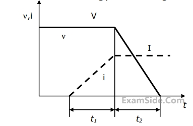
The figure shows a straight-line approximation for the forward characteristics of a power diode. A continuous on-state current of 15 A is flowing through the diode.

What is the power loss in the diode?
Consider the circuit shown in Figure (a). A gate pulse $v_g$ is applied between time instants $t_0$ and $t_1$. After $t_1$, during the MOSFET turn OFF process, it experiences a voltage overshoot.


Based on the $v_{d s}$ waveforms shown in Figure (b), which one of the following options is correct?
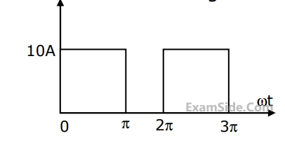
If the following switching devices have similar power ratings, which one of them is the fastest?
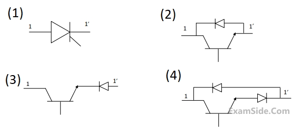
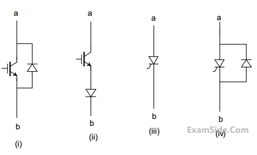
A semiconductor switch needs to block voltage V of only one polarity (V > 0) during OFF state as shown in figure (i) and carry current in both directions during ON state as shown in figure (ii). Which of the following switch combination(s) will realize the same?

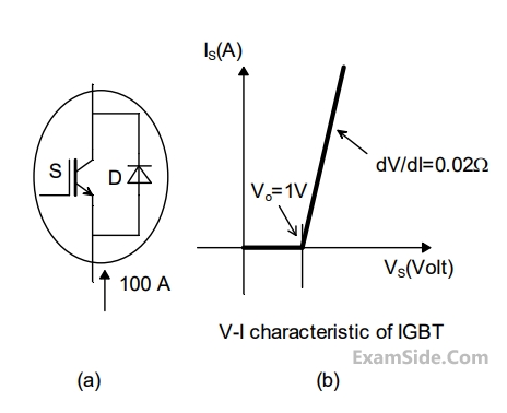
A charger supplies 100 W at 20 V for charging the battery of a laptop. The power devices, used in the converter inside the charger, operate at a switching frequency of 200 kHz. Which power device is best suited for this purpose?


Marks 2


The minimum approximate volt $$-$$second rating of the pulse transformer suitable for triggering the $$SCR$$ should be: (Volt - second rating is the maximum of product of the voltage and the width of the pulse that may be applied)
The resistance $$R$$ should be


Which of the following are valid realizations of the switch $$s$$?