Marks 1
1
If $${X_1}$$ and $${X_2}$$ are the inputs to the circuit shown in the figure, the output $$Q$$ is

GATE EE 2005
2
In standard $$TTL$$ gates, the totem pole output stage is primarily used to
GATE EE 1998
3
The open collector outputs of two$$2$$-inputs $$NAND$$ gates are connected to a common pull up resistor. If the input to the gates are $$P,Q$$ and $$R,S$$ respectively, the output is equal to
GATE EE 1998
Marks 2
1
The MOSFET switches shown in the circuit are ideal.
Which of the following is the correct option for Boolean logical expression of the output (OUT), and the maximum possible power (P) consumed by the circuit?
GATE EE 2026
2
The $$TTL$$ circuit shown in the figure is fed with the waveform $$X$$ (also shown). All gates have equal propagation delay of $$10$$ $$ns.$$ The output $$Y$$ of the circuit is


GATE EE 2010
3
A TTL NOT gate circuit is shown in figure. Assuming $${V_{BE}} = 0.7\,v$$ of both the transistors, if $${V_i} = 3.0\,V,$$ then the states of the two transistors will be
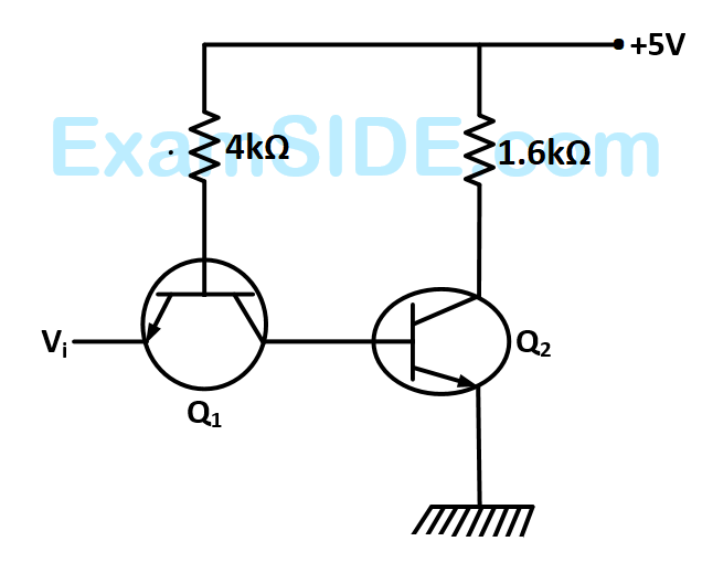
GATE EE 2006