Analog to Digital and Digital to Analog Converter · Digital Electronics · GATE EE
Marks 1
1
The voltage comparator shown in Fig. can be used in the analog-to-digital conversion as

GATE EE 2004
2
Among the following four, the slowest $$ADC$$ (analog-to-digital converter) is
GATE EE 2001
3
The number of comparisons carried out in a $$4$$-bit flash type $$A/D$$ converter is
GATE EE 1994
4
A $$10$$ bit $$A/D$$ converter is used to digitize an analog signal in the $$0$$ to $$5$$ $$V$$ range. The maximum peak to peak ripple voltage that can be allowed in the $$D.C.$$ supply voltage is
GATE EE 1993
Marks 2
1
An 8 bit ADC converts analog voltage in the range of 0 to +5 V to the corresponding digital code as per the conversion characteristics shown in figure. For $$V_{in}=1.9922~V$$, which of the following digital output, given in hex, is true?

GATE EE 2023
2
A $$2$$-bit flash Analog to Digital Converter $$(ADC)$$ is given below. The input is $$0 \le {V_N} \le 3$$ Volts. The expression for the $$LSB$$ of the output $${B_0}$$ as Boolean function of $${X_2},\,{X_1}$$ and $${X_0}$$ is

GATE EE 2016 Set 1
3
An $$8$$-bit, unipolar Successive Approximation Register type $$ADC$$ is used to convert $$3.5$$ $$V$$ to digital equivalent output. The reference voltage is $$+5 V.$$ The output of the $$ADC,$$ at the end of $$3$$rd clock pulse after the start of conversion, is
GATE EE 2015 Set 1
4
A student has made a-$$3$$ bit binary down counter and connected to the $$R$$-$$2R$$ ladder type $$DAC$$ [Gain $$=$$ $$\left( { - 1k\Omega /2R} \right)$$ as shown in figure to generate a staircase waveform.
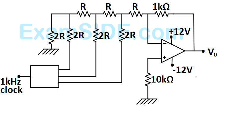
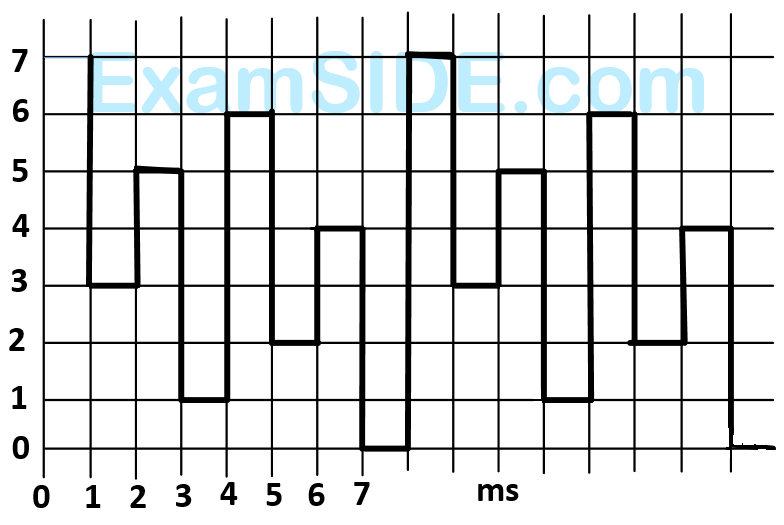
The output achieved is different as shown in figure. What could be the possible cause of this error?
GATE EE 2006
5
A digital-to-analog converter with a full -scale output voltage of $$3.5$$ $$V$$ has a resolution close to $$14$$ $$m$$ $$V.$$ Its bit size is
GATE EE 2005
6
The simplified block diagram of a $$10$$-bit $$A/D$$ converter of dual slope integrator type is shown in Fig. The $$10$$-bit counter at the output is clocked by a $$1$$ $$MHz$$ clock. Assuming negligible timing overhead for the control logic, the maximum frequency of the analog signal that can be converted using this $$A/D$$ converter is approximately. Input sample to be converter

GATE EE 2003
7
For a dual $$ADC$$ type $$3\,{\raise0.5ex\hbox{$\scriptstyle 1$}
\kern-0.1em/\kern-0.15em
\lower0.25ex\hbox{$\scriptstyle 2$}}$$ digit $$DVM$$, the reference voltage is $$100$$ $$mV$$ and the first integration time is set to $$300$$ $$ms$$. For some input voltage, the ''deintegration'' period is $$370.2ms.$$ The $$DVM$$ will indicate.
GATE EE 1999