Operational Amplifier · Analog Electronics · GATE EE
Marks 1
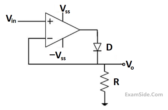
$$ \text { Assuming ideal op-smps, the circuit represents is } $$

The steady state output (Vout), of the circuit shown below, will

P. $$\,\,\,\,$$High common mode rejection ratio
Q. $$\,\,\,\,$$High input impedance
R. $$\,\,\,\,$$High linearity
S. $$\,\,\,\,$$High output impedance


The cut-off frequencies of $$F1$$ and $$F2$$ are $${f_1}$$ and $${f_2}$$ respectively. If $${f_1}\, < \,{f_2},$$ the resultant circuit exhibits the characteristic of a

The output of the circuit for a given input $${V_i}$$ is


Marks 2
$$ \text { In the circuit shown, the open loop gain of the operational amplifier is } A_0=105 \text {. } $$

$$ \text { What is the voltage gain of the circuit? (Round off to two decimal places) } $$
In the circuit, shown below, if the values of $R$ and $C$ are very large, the form of the output voltage for a very high frequency square wave input, is best represented by

The op-amps in the following circuit are ideal. The voltage gain of the circuit is ___________. (Round off to the nearest integer)

A difference amplifier is shown in the figure. Assume the op-amp to be ideal. The CMRR (in dB) of the difference amplifier is ________ (rounded off to 2 decimal places).

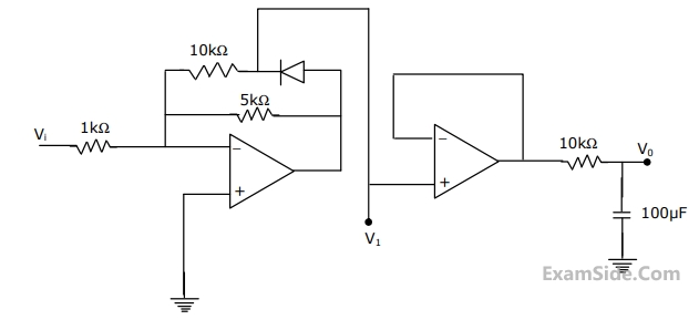
Consider the OP AMP based circuit shown in the figure. Ignore the conduction drops of diodes $$D_1$$ and $$D_2$$. All the components are ideal and the breakdown voltage of the Zener is 5 V. Which of the following statements is true?

The output impedance of a non-ideal operational amplifier is denoted by Zout. The variation in the magnitude of Zout with increasing frequency, f, in the circuit shown below, is best represented by

The current gain (Iout/Iin) in the circuit with an ideal current amplifier given below is


Which one of the following is TRUE?


If the lower and upper trigger level voltages are $$0.9$$ $$V$$ and $$1.7$$ $$V,$$ the period (in $$ms$$), for which output is LOW, is ____________.


It is desired to make full wave rectifier using two half wave rectifiers. The resultant circuit will be

If $${R_1} = {R_2} = {R_A}$$ and $${R_3} = {R_4} = {R_B},$$ the circuit acts as a

If the voltage $${v_1}$$ is made $$+2.5$$ $$V,$$ the voltage waveform at $$'P'$$ will become.
The output of the filter in above is given to the circuit shown in figure The gain $${V_S}$$ frequency characteristic of the $$0/p$$ $$\left( {{V_0}} \right)$$ will be


$$T\left( s \right) = {{{{ - s} \over {\left( {{R_1}C} \right)}}} \over {{s^2} + {{2s} \over {\left( {{R_3}C} \right)}} + {1 \over {\left( {R{R_3}{C^2}} \right)}}}}$$
where, $$R = {R_1}||{R_2}$$
If $${R_1} = 2k\Omega ,{R_2} = 2/3\,k\Omega ,\,\,{R_3} = 200\,k\Omega $$ and $$C = 0.1\,\,\mu F,$$ determine the center frequency $${\omega _0},$$ gain $${A_0}$$ and the $$Q$$ of the filter.
List - $${\rm I}$$ (Circuit)


List - $${\rm II}$$ (Functions)
$$(P)$$$$\,\,\,\,\,$$ High-pass filter
$$(Q)$$$$\,\,\,\,\,$$ Amplifier
$$(R)$$$$\,\,\,\,\,$$ Comparator
$$(S)$$$$\,\,\,\,\,$$ Low-pass filter


$${{{d^2}V} \over {d{t^2}}} + a.{{dV} \over {dt}} + bV = f\left( t \right).$$
Find $$a,b$$ and $$f(t)$$


Marks 5


$${R_i} = 100\,k\Omega ,\,\,{R_0} = 50\,k\Omega .$$ For $${V_0} = 10V.$$
Calculate $${V_S}$$ and $${{{V_0}} \over {{V_S}}}$$ and estimate the input resistance of the circuit,


$$(i)$$ Calculate the transfer function $${{{V_0}} \over {{V_i}}}$$
$$(ii)$$ plot the amplitude and phase response as a function for $$R = {R_1}$$
$$(a)$$ Draw the equivalent circuit and evaluate the gain $$\left( {{V_0}\,\,vs\,\,{V_i}} \right)$$ of the circuit for

$$(i)$$ $${V_i} \le 0$$ $$\,\,\,\,\,\left( {ii} \right)\,\,\,0 < {V_i} < 5V\,\,\,\,\,\,$$ $$\,\,\,\,\,\left( {iii} \right)\,\,\,{V_i} > 5V\,\,\,\,\,\,$$
$$(b)$$ Sketch the gain $$\left( {{V_0}\,\,\,{V_s}\,\,\,{V_i}} \right)$$ characteristics of the above circuit and label the salient features.