1
GATE ECE 2017 Set 1
MCQ (Single Correct Answer)
+1
-0.3
Consider a wireless communication link between a transmitter and a receiver located in free space, with finite and strictly positive capacity. If the effective areas of the transmitter and the receiver antennas, and the distance between them are all doubled, and everything else remains unchanged, the maximum capacity of the wireless link
2
GATE ECE 2017 Set 1
Numerical
+2
-0
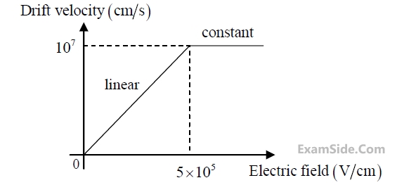
The dependence of drift velocity of electrons on electric field in a semiconductor is shown
below. The semiconductor has a uniform electron concentration of n = 1x10¹⁶ $$cm^{-3}$$ and electronic charge q = 1.6x10⁻¹⁹ C. If a bias of 5V is applied across a 1 $$\mu$$m region of this
semiconductor, the resulting current density in this region, in kA/cm2, is _________.
Your input ____
3
GATE ECE 2017 Set 1
MCQ (Single Correct Answer)
+1
-0.3
A bar of Gallium Arsenide (GaAs) is doped with Silicon such that the Silicon atoms occupy
Gallium and Arsenic sites in the GaAs crystal. Which one of the following statement is true?
4
GATE ECE 2017 Set 1
MCQ (Single Correct Answer)
+1
-0.3
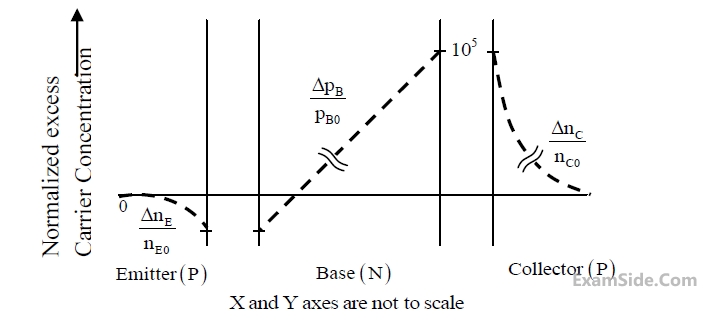
For a narrow base PNP BJT, the excess minority carrier concentration ($$\bigtriangleup n_E$$ for emitter,
$$\bigtriangleup p_B$$ for base, $$\bigtriangleup n_E$$ for collector) normalized to equilibrium minority carrier concentration
($$\bigtriangleup n_{E0}$$ for emitter, $$\bigtriangleup p_{B0}$$ for base, $$\bigtriangleup n_{C0}$$ for collector) in the quasi-neutral emitter, base and collector
regions are shown below. Which one of the following biasing modes is the transistor operating in?
Paper Analysis
Total Questions
Analog Circuits 5
Communications 5
Control Systems 6
Digital Circuits 5
Electromagnetics 5
Electronic Devices and VLSI 4
Engineering Mathematics 10
Microprocessors 2
Network Theory 3
Signals and Systems 7
General Aptitude 10
More Papers of GATE ECE
GATE ECE 2026 GATE ECE 2025 GATE ECE 2024 GATE ECE 2023 GATE ECE 2022 GATE ECE 2021 GATE ECE 2020 GATE ECE 2019 GATE ECE 2018 GATE ECE 2017 Set 2 GATE ECE 2017 Set 1 GATE ECE 2016 Set 2 GATE ECE 2016 Set 1 GATE ECE 2016 Set 3 GATE ECE 2015 Set 3 GATE ECE 2015 Set 2 GATE ECE 2015 Set 1 GATE ECE 2014 Set 1 GATE ECE 2014 Set 4 GATE ECE 2014 Set 2 GATE ECE 2014 Set 3 GATE ECE 2013 GATE ECE 2012 GATE ECE 2011 GATE ECE 2010 GATE ECE 2009 GATE ECE 2008 GATE ECE 2007 GATE ECE 2006 GATE ECE 2005 GATE ECE 2004 GATE ECE 2003 GATE ECE 2002 GATE ECE 2001 GATE ECE 2000 GATE ECE 1999 GATE ECE 1998 GATE ECE 1997 GATE ECE 1996 GATE ECE 1995 GATE ECE 1994 GATE ECE 1993 GATE ECE 1992 GATE ECE 1991 GATE ECE 1990 GATE ECE 1989 GATE ECE 1988 GATE ECE 1987
GATE ECE Papers
All year-wise previous year question papers
2026
2025
2024
2023
2022
2021
2020
2019
2018
2013
2012
2011
2010
2009
2008
2007
2006
2005
2004
2003
2002
2001
2000
1999
1998
1997
1996
1995
1994
1993
1992
1991
1990
1989
1988
1987