1
GATE EE 2003
MCQ (Single Correct Answer)
+2
-0.6
The following equation defines a separately exited $$dc$$ motor in the form of a differential equation $${{{d^2}\omega } \over {d{t^2}}} + {{B\,d\omega } \over {j\,\,dt}} + {{{K^2}} \over {LJ}}\omega = {K \over {LJ}}{V_a}$$
The above equation may be organized in the state space form as follows
$$\left( {\matrix{
{{{{d^2}\omega } \over {d{t^2}}}} \cr
{{{d\omega } \over {dt}}} \cr
} } \right) = P\left( {\matrix{
{{{d\omega } \over {dt}}} \cr
\omega \cr
} } \right) + Q{V_a}$$
where the $$P$$ matrix is given by
2
GATE EE 2003
MCQ (Single Correct Answer)
+1
-0.3
A lead compensator used for a closed loop controller has the following transfer function $${\textstyle{{K\left( {1 + {s \over a}} \right)} \over {\left( {1 + {s \over b}} \right)}}}\,\,\,$$ For such a lead compensator
3
GATE EE 2003
MCQ (Single Correct Answer)
+1
-0.3
A second order system starts with an initial condition of $$\left( {\matrix{
2 \cr
3 \cr
} } \right)$$ without any external input. The state transition matrix for the system is given by $$\left( {\matrix{
{{e^{ - 2t}}} & 0 \cr
0 & {{e^{ - t}}} \cr
} } \right).$$ The state of the system at the end of $$1$$ second is given by.
4
GATE EE 2003
MCQ (Single Correct Answer)
+2
-0.6
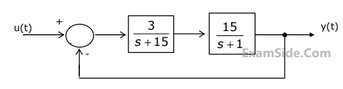
The roots of the closed loop characteristic equation of the system shown in fig is
Paper Analysis
Total Questions
Analog Electronics 8
Control Systems 10
Digital Electronics 5
Electric Circuits 10
Electrical and Electronics Measurement 10
Electrical Machines 14
Electromagnetic Fields 4
Power Electronics 7
Power System Analysis 17
More Papers of GATE EE
GATE EE 2026 GATE EE 2025 GATE EE 2024 GATE EE 2023 GATE EE 2022 GATE EE 2021 GATE EE 2020 GATE EE 2019 GATE EE 2018 GATE EE 2017 Set 2 GATE EE 2017 Set 1 GATE EE 2016 Set 1 GATE EE 2016 Set 2 GATE EE 2015 Set 1 GATE EE 2015 Set 2 GATE EE 2014 Set 3 GATE EE 2014 Set 2 GATE EE 2014 Set 1 GATE EE 2013 GATE EE 2012 GATE EE 2011 GATE EE 2010 GATE EE 2009 GATE EE 2008 GATE EE 2007 GATE EE 2006 GATE EE 2005 GATE EE 2004 GATE EE 2003 GATE EE 2002 GATE EE 2001 GATE EE 2000 GATE EE 1999 GATE EE 1998 GATE EE 1997 GATE EE 1996 GATE EE 1995 GATE EE 1994 GATE EE 1993 GATE EE 1992 GATE EE 1991
GATE EE Papers
All year-wise previous year question papers
2026
2025
2024
2023
2022
2021
2020
2019
2018
2013
2012
2011
2010
2009
2008
2007
2006
2005
2004
2003
2002
2001
2000
1999
1998
1997
1996
1995
1994
1993
1992
1991