1
GATE EE 2003
MCQ (Single Correct Answer)
+2
-0.6
Assuming the operational amplifier to be ideal, the gain $${V_{out}}/{V_{in}}$$ for the circuit shown in figure

2
GATE EE 2003
MCQ (Single Correct Answer)
+2
-0.6
The circuit of fig shows a $$555$$ Timer $$IC$$ connected as an Astable multivibrator. The value of the capacitor $$C$$ is $$10$$ $$nF.$$ The values of the resistors $${R_A}$$ and $${R_B}$$ for a frequency of $$10$$ $$kHz$$ and a duty cycle of $$0.75$$ for the output voltage waveform are

3
GATE EE 2003
MCQ (Single Correct Answer)
+1
-0.3
The variation of drain current with gate-to-source voltage $$\left( {{{\rm I}_D} - {V_{GS}}} \right.$$ characteristic$$\left. \, \right)$$ of a MOSFET is shown in Figure. The MOSFET is

4
GATE EE 2003
MCQ (Single Correct Answer)
+1
-0.3
In the circuit of figure shown, assume that the transistor has $${h_{fe}} = 99$$ and $${V_{BE}} = 0.7V.$$
The value of collector current $${{\rm I}_C}$$ of the transistor is approximately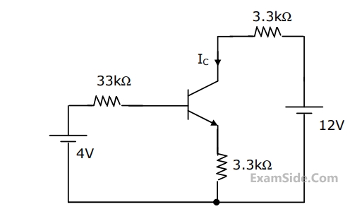
The value of collector current $${{\rm I}_C}$$ of the transistor is approximately
Paper Analysis
Total Questions
Analog Electronics 8
Control Systems 10
Digital Electronics 5
Electric Circuits 10
Electrical and Electronics Measurement 10
Electrical Machines 14
Electromagnetic Fields 4
Power Electronics 7
Power System Analysis 17
More Papers of GATE EE
GATE EE 2026 GATE EE 2025 GATE EE 2024 GATE EE 2023 GATE EE 2022 GATE EE 2021 GATE EE 2020 GATE EE 2019 GATE EE 2018 GATE EE 2017 Set 2 GATE EE 2017 Set 1 GATE EE 2016 Set 1 GATE EE 2016 Set 2 GATE EE 2015 Set 1 GATE EE 2015 Set 2 GATE EE 2014 Set 3 GATE EE 2014 Set 2 GATE EE 2014 Set 1 GATE EE 2013 GATE EE 2012 GATE EE 2011 GATE EE 2010 GATE EE 2009 GATE EE 2008 GATE EE 2007 GATE EE 2006 GATE EE 2005 GATE EE 2004 GATE EE 2003 GATE EE 2002 GATE EE 2001 GATE EE 2000 GATE EE 1999 GATE EE 1998 GATE EE 1997 GATE EE 1996 GATE EE 1995 GATE EE 1994 GATE EE 1993 GATE EE 1992 GATE EE 1991
GATE EE Papers
All year-wise previous year question papers
2026
2025
2024
2023
2022
2021
2020
2019
2018
2013
2012
2011
2010
2009
2008
2007
2006
2005
2004
2003
2002
2001
2000
1999
1998
1997
1996
1995
1994
1993
1992
1991