1
GATE ECE 2016 Set 3
MCQ (Single Correct Answer)
+1
-0.3
The figure shows the band diagram of a Metal Oxide Semiconductor (MOS). The surface region of
this MOS is in

2
GATE ECE 2016 Set 3
Numerical
+2
-0
Figures $${\rm I}$$ and $${\rm I}{\rm I}$$ show two MOS capacitor of unit area. The capacitor in Figure I has insulator materials X (of thickness t1 = 1 nm and dielectric constant $${\varepsilon _1}$$ = 4) and Y (of thickness t2 =3 nm and dielectric constant $${\varepsilon _2}$$ = 200). The capacitor in Figure $${\rm I}{\rm I}$$ has only insulator material X of thickness teq. If the capacitors are of equal capacitance, then the value of teq (in nm) is ______


Your input ____
3
GATE ECE 2016 Set 3
Numerical
+2
-0
In the circuit shown in the figure, transistor M1 is in saturation and has transconductance
gm = 0.01 siemens. Ignoring internal parasitic capacitances and assuming the channel length
modulation $$\lambda $$ to be zero, the small signal input pole frequency (in kHz) is _____
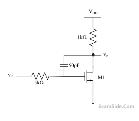
Your input ____
4
GATE ECE 2016 Set 3
MCQ (Single Correct Answer)
+2
-0.6
In the circuit shown in the figure, the channel length modulation of all transistors is non-zero $$\left( {\lambda \ne 0} \right)$$. Also all transistors operate in saturation and have negligible body effect. The ac small
signal voltage gain $$\left( {{V_0}/{V_{in}}} \right)$$ of the circuit is

Paper Analysis
Total Questions
Analog Circuits 4
Communications 6
Control Systems 5
Digital Circuits 3
Electromagnetics 5
Electronic Devices and VLSI 7
Engineering Mathematics 9
Microprocessors 1
Network Theory 4
Signals and Systems 6
General Aptitude 2
More Papers of GATE ECE
GATE ECE 2026 GATE ECE 2025 GATE ECE 2024 GATE ECE 2023 GATE ECE 2022 GATE ECE 2021 GATE ECE 2020 GATE ECE 2019 GATE ECE 2018 GATE ECE 2017 Set 1 GATE ECE 2017 Set 2 GATE ECE 2016 Set 1 GATE ECE 2016 Set 2 GATE ECE 2016 Set 3 GATE ECE 2015 Set 3 GATE ECE 2015 Set 1 GATE ECE 2015 Set 2 GATE ECE 2014 Set 1 GATE ECE 2014 Set 3 GATE ECE 2014 Set 4 GATE ECE 2014 Set 2 GATE ECE 2013 GATE ECE 2012 GATE ECE 2011 GATE ECE 2010 GATE ECE 2009 GATE ECE 2008 GATE ECE 2007 GATE ECE 2006 GATE ECE 2005 GATE ECE 2004 GATE ECE 2003 GATE ECE 2002 GATE ECE 2001 GATE ECE 2000 GATE ECE 1999 GATE ECE 1998 GATE ECE 1997 GATE ECE 1996 GATE ECE 1995 GATE ECE 1994 GATE ECE 1993 GATE ECE 1992 GATE ECE 1991 GATE ECE 1990 GATE ECE 1989 GATE ECE 1988 GATE ECE 1987
GATE ECE Papers
All year-wise previous year question papers
2026
2025
2024
2023
2022
2021
2020
2019
2018
2013
2012
2011
2010
2009
2008
2007
2006
2005
2004
2003
2002
2001
2000
1999
1998
1997
1996
1995
1994
1993
1992
1991
1990
1989
1988
1987