PN Junction · Electronic Devices and VLSI · GATE ECE
Marks 1


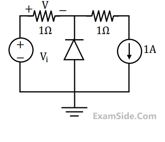
The maximum and minimum values of the output voltage respectively are
Marks 2
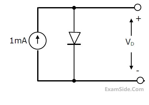
The photocurrent of a PN junction diode solar cell is 1 mA. The voltage corresponding to its maximum power point is 0.3 V. If the thermal voltage is 30 mV, the reverse saturation current of the diode (in nA, rounded off to two decimal places) is _____.
A p-type semiconductor with zero electric field is under illumination (low level injection) in steady state condition. Excess minority carrier density is zero at x = $$\pm$$ 2ln, where ln = 10$$-$$4 cm is the diffusion length of electrons. Assume electronic charge, q = $$-$$1.6 $$\times$$ 10$$-$$19 C. The profiles of photo-generation rate of carriers and the recombination rate of excess minority carriers (R) are shown. Under these conditions, the magnitude of the current density due to the photo-generated electrons at x = +2ln is ___________ mA/cm2 (rounded off to two decimal places).


Given q = 1.6 × 10⁻¹⁹ coulomb, $$\varepsilon$$0 = 8.85 × 10⁻¹⁴ F/cm, $$\varepsilon$$r = 11.7 for silicon, the value of L in nm is ________.


(Give the sketch showing the magnitudes of the current at t = 0, t = t0 and t = $$\infty$$ )
