Semiconductor Devices and Logic Gates · Physics · COMEDK
MCQ (Single Correct Answer)
Pick out the correct statement from the following;
What is the minimum wavelength of radiation required to detect a p-n junction diode made of a semiconductor having band gap 3.3 eV .
[Planck's constant $h=6.6 \times 10^{34} \mathrm{~J} . \mathrm{s}$ ]
Find the current through the $40 \Omega$ resistor in the given circuit having a diode, three resistors and two cells.

In a PN junction diode, the forward bias is increased gradually from 0 Volt to 1 Volt. Which of the following statements is correct?
A. The depletion width increases, and barrier potential increases
B. The depletion width decreases, but the electric field inside the junction increases
C. The depletion width remains unchanged, but current increases
D. The depletion width decreases and barrier potential decreases
A silicon sample is doped simultaneously with donor impurity phosphorus at a concentration of $N_D=3 \times 10^{22} \mathrm{~m}^{-3}$ and acceptor impurity boron at a concentration of $N_D=2.8 \times 10^{22} \mathrm{~m}^{-3}$. The intrinsic carrier concentration of silicon at room temperature is $n_i=1.5 \times 10^{16} \mathrm{~m}^{-3}$. Assuming complete ionization, the hole concentration is :

In the circuit given, the reverse breakdown voltage of the Zener diode is 4.8 V . The current through the Zener and the power dissipation in Zener is:
The zener voltage in the circuit shown is $\mathrm{V}_{\mathrm{Z}}=20 \mathrm{~V}$. The load resistance $\mathrm{R}_{\mathrm{L}}=5 \mathrm{k} \Omega$ and the resistance $\mathrm{R}_{\mathrm{S}}=10 \mathrm{k} \Omega$. If the input voltage is $\mathrm{V} \mathrm{s}=100 \mathrm{~V}$, then the current through the zener diode in milliampere is:


Three ideal diodes and resistors connected to the cell of negligible internal resistance is as shown. Find the current passing through the $10 \Omega$ resistor.
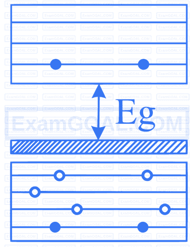
In the energy band diagram of a material shown below, open circles and filled circles denote holes and electrons respectively. The material is a
The conductivity of a semiconductor increases with increase in temperature because
A) number density of free current carriers increases
B) relaxation time increases
C) both number density of carriers and relaxation time increase
D) number density of current carriers increases, relaxation time decreases but effect of decrease in relaxation time is much less than increase in number density

The output of the given circuit is
A. Negatively rectified half wave
B. Positively rectified half wave
C. Negatively rectified full wave
D. Zero all times
The following are the graphs of potential barrier versus width of the depletion region for a p-n junction diode.

Which of the following is correct?
| I | II | III | IV` |
|---|---|---|---|
| A - unbiased diode | A - Forward biased diode | A - unbiased diode | A - unbiased diode |
| B - Reverse biased | B - Reverse biased | B - Forward biased | B - unused diode |
| C - Forward biased | C - unbiased | C - Reverse biased | C - Forward biased |
$$ \text { In a p-n junction, the depletion layer of thickness } 1 \mu \mathrm{m} \text { has } 0.05 \mathrm{~V} \text { potential across it. The electric field in } N C^{-1} \text { is } $$
The mobility of the charge carriers increases with
In intrinsic semiconductors at room temperature, number of electrons and holes are
A semiconductor $$\mathrm{X}$$ is made by doping silicon with phosphorous. A second semiconductor $$\mathrm{Y}$$ is made by doping silicon with aluminium. The two are joined by a suitable technique to form a $$\mathrm{p}$$-$$\mathrm{n}$$ junction and is connected to a battery such that $$\mathrm{Y}$$ is joined to negative of the battery and $$\mathrm{X}$$ to the positive of the battery. Which of the following statements is correct?
In a given semiconductor, the ratio of the number density of electron to number density of hole is $$2: 1$$. If $$\frac{1}{7}$$th of the total current is due to the hole and the remaining is due to the electrons, the ratio of the drift velocity of holes to the drift velocity of electrons is :
An ideal diode is connected in series with a capacitor. The free ends of the capacitor and the diode are connected across a $$220 \mathrm{~V}$$ ac source. Now the potential difference across the capacitor is :
Though $$\mathrm{Sn}$$ and $$\mathrm{Si}$$ are $$4^{\text {th }}$$ group elements, $$\mathrm{Sn}$$ is a metal while $$\mathrm{Si}$$ is a semiconductor because
A transistor is connected in CE configuration. The collector supply is $$10 \mathrm{~V}$$ and the voltage drop across a resistor of $$1000 \Omega$$ in the collector circuit is $$0.5 \mathrm{~V}$$. If the current gain factor is 0.96 , then the base current is
Which logic gate is represented by the following combination logic gates?

An LED is constructed from a $$p$$-$$n$$ junction diode using GaAsP. The energy gap is $$1.9 \mathrm{~eV}$$. The wavelength of the light emitted will be equal to
The energy gap between valance band and the conduction band for a given material is $$6 \mathrm{~eV}$$, then the material is :
In the given circuit the diode $$D_1$$ and $$D_2$$ have the forward resistance $$25 \Omega$$ and infinite backward resistance. When they are connected to the source as shown, the current passing through the $$175 \Omega$$ resistor is:

The reverse current in the semiconductor diode changes from $$20 \mu \mathrm{A}$$ to $$40 \mu \mathrm{A}$$ when the reverse potential is changed from $$10 \mathrm{~V}$$ to $$15 \mathrm{~V}$$, then the reverse resistance of the junction diode will be :
For CE transistor amplifier, the audio signal voltage across the collector resistance of 4 k$$\Omega$$ is 5 V. If the current amplification factor of the transistor is 100 and base resistance is 2 k$$\Omega$$, then input signal voltage is
Which of the following gate give the similar output as the output of circuit diagram shown in the figure?

Choose the incorrect statements.
Find the logic gate, when both the inputs are high but the output is low and vice-versa.
What is the minimum band-gap of the LED diode?
When a $$p$$-$$n$$ junction diode is connected in forward bias, its barrier potential