Semiconductor Devices and Logic Gates · Physics · KCET
MCQ (Single Correct Answer)

The circuit shown in figure contains two ideal diodes $D_1$ and $D_2$. If a cell of emf $3 V$ and negligible internal resistance is connected as shown, then the current through $70 \Omega$ resistance, (in ampere) is

Depletion region in an unbiased semiconductor diode is a region consisting of only free electrons only holes
The upper level of valence band and lower level of conduction band overlap in the case of
In the diagram shown, the Zener diode has a reverse breakdown voltage of $V_Z$. The current through the load resistance $R_L$ is $I_L$. The current through the Zener diode is

A $p-n$ junction diode is connected to a battery of emf 5.7 V in series with a resistant $5 \mathrm{k} \Omega$ such that it is forward biased. If the barrier potential of the diode is 0.7 V , neglecting the diode resistance, the current in the circuit is
When a $$p$$-$$n$$ junction diode is in forward bias, which type of charge carriers flows in the connecting wire?
A full-wave rectifier with diodes $$D_1$$ and $$D_2$$ is used to rectify $$50 \mathrm{~Hz}$$ alternating voltage. The diode $$D_1$$ conducts ......... times in one second.
A truth table for the given circuit is

The resistivity of a semiconductor at room temperature is in between
The forbidden energy gap for Ge crystal at 0K is
Which logic gate is represented by the following combination of logic gates?

The circuit given represents which of the logic operations?

Identify the incorrect statement.
Three photodiodes $$D_1, D_2$$ and $$D_3$$ are made of semiconductors having band gaps of $$2.5 \mathrm{~eV}, 2 \mathrm{~eV}$$ and $$3 \mathrm{~eV}$$, respectively. Which one will be able to detect light of wavelength $$600 \mathrm{~nm}$$ ?
In the following circuit what are P and Q

A positive hole in a semiconductor is
The conductivity of semiconductor increases with increase in temperature because
For a transistor amplifier, the voltage gain
In the following circuit, what are P and Q?

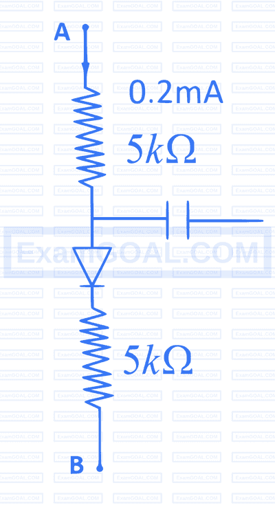
In the figure shown, if the diode forward voltage drop is 0.2 V , the voltage difference between $A$ and $B$ is